
Wireless Communication PCB: Breaking the Myth of Premium Materials for Better RF Performance
Many assume that wireless communication PCBs require expensive high-frequency materials. This guide
Hardware Is the Foundation. The Real Question Is What We Build on Top of It.
Every time I look at those neatly arranged server motherboards inside equipment racks, I find myself wondering whether we have over-mystified this hardware. Everyone talks about how high multi-layer PCBs carry the flood of computational power — as though those copper foil traces are the neural pathways of artificial intelligence. But I think this framing is slightly backwards. What truly drives AI evolution has never been how precise a circuit board is — it is what specific problems we are trying to solve with it.
I have encountered plenty of project teams that immediately pursue the most premium server configurations, opening conversations with questions about how many layers of Server Motherboard PCB can support how many PCIe lanes. It is as though stacking hardware specifications has become a kind of technical competition. But when systems actually run, the bottlenecks in complex models almost always appear in the data pipeline or algorithm optimization — not in whether the motherboard can transmit signals slightly faster.
The Silent Collaborator That Keeps Thinking Possible
That said, I am not dismissing hardware. High multi-layer PCB design is genuinely an art form — it requires balancing power noise, signal crosstalk, and thermal dissipation within extremely constrained space. But this is more of a triumph of fundamental engineering than anything magical. What is actually fascinating is how we use these stable, reliable foundations to build unstable, unpredictable intelligence.
I prefer to think of the server motherboard as a silent collaborator. It does not participate in thinking — but it ensures that thinking can keep happening. When you are training a large language model, the electrical signals flowing inside the PCB have no idea whether they represent Shakespeare or software instructions. They simply and faithfully complete their physical-layer transmission tasks. This determinism stands in remarkable contrast to the fundamental uncertainty of the AI models operating above it.
Much of the current discussion has artificially separated AI hardware and software — as though one group of PCB engineers is relentlessly adding layers while an entirely separate group of algorithm researchers designs new architectures in a parallel universe. But I believe the real breakthroughs will emerge precisely at the intersection. When hardware design begins to understand software requirements, and when algorithm development begins to account for hardware constraints, truly elegant solutions start to appear.
A friend doing computer vision work once told me that their team, in order to reduce latency, redesigned how data flowed between multiple GPUs. They found that adjusting the task scheduling strategy was far more effective than pursuing a higher-specification motherboard interconnect. That experience made me realize: sometimes the technical specifications we chase are nothing more than a mirage.
So when I see news about PCB layer counts reaching new records, my reaction is to wonder: does this mean we have not done enough at the software layer? If we need increasingly complex physical structures to support intelligence, is that intelligence itself perhaps too unwieldy? Perhaps the true AI revolution will not happen between 38 layers of copper foil — but in the instant when a developer suddenly understands something fundamental. And at that moment, perhaps even the form factor of a server will change.
A Server Motherboard Is Nothing Like a Desktop Motherboard
I always feel that many people misunderstand server motherboards. They seem to think it is just a scaled-up version of a desktop computer motherboard. The reality is entirely different. If you disassemble an ordinary home computer, that motherboard is relatively simple — just a few layers, with a fairly straightforward design philosophy. But when you are facing a server motherboard designed for a data center or AI training system, the feeling is completely different. It is more like a miniaturized city, where every road, pipeline, and power grid must be precisely planned within an extremely compact space.
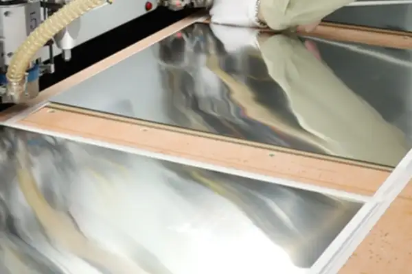
Take the PCB — the circuit board carrying all of the chips. In high-end servers, particularly those running AI models, the complexity of this board increases at a geometric rate. It is no longer a simple few-layer structure — it routinely uses dozens of layers in a complex laminate stack. What we commonly call the “high multi-layer PCB” is exactly this. Each layer is not randomly stacked — how signal layers are routed, how power layers are distributed, how ground planes are arranged, everything serves a single core objective: ensuring that signals travel cleanly and accurately from point A to point B.
Consider that chip-to-chip data transfer rates today are staggering — streams of hundreds of gigabits per second racing through copper traces thinner than a human hair. In this environment, any interference is potentially catastrophic. A board material with slightly too much loss; a via design that leaves even a tiny unnecessary “stub”; even microdeformation of the board under temperature variation — these seemingly insignificant details can all cause data errors. Making a qualified Server Motherboard PCB is far from simple “printed circuitry.” It is a discipline that fuses materials science, electromagnetic theory, and precision manufacturing.
Many people feel the cost is unreasonably high: it is just a board, right? But its value lies precisely in what is invisible. To pursue extreme signal integrity (SI) and power integrity (PI), engineers must specify expensive low-loss base materials and high-performance copper foil. Machining precision requirements are stringent to the micrometer level. This drives costs to levels entirely incomparable with ordinary consumer products.
I have seen many projects that chose a poorly suited PCB solution or manufacturer early on to save a little money — and paid dearly for it later. Systems became unstable, debugging pushed teams to the edge, and in the end the money and time spent far exceeded whatever was saved upfront.
A good server motherboard PCB is the silent cornerstone. It does not directly participate in computation, but it determines whether computation can proceed stably, efficiently, and persistently. In this era, the performance ceiling of hardware is very often defined by these most foundational “soil conditions.”
Layer Count Is a Means, Not a Goal
I have always felt that many people’s thinking about high-end server motherboard PCBs drifts toward surface-level parameters — fixating on specifications that sound impressive but may miss what actually matters. The real critical factors are often hidden in the most fundamental manufacturing steps.
Take something as basic as fiberglass cloth. When high-performance substrate materials come up in industry conversation, everyone loves to discuss Low-Dk or various new resin systems — which is certainly valid — but I think the stability of the base material itself is dramatically undervalued. Consider: a High multi-layer PCB with dozens of layers uses enormous quantities of fiberglass cloth across its structure. The flatness and uniformity of every layer quietly determines the upper bound of final performance. Weaving density, yarn diameter, and surface treatment process directly determine the dielectric constant stability and coefficient of thermal expansion after the cloth bonds with resin. Processes like open-fiber treatment or flat-yarn glass cloth provide more uniform resin wet-out and thinner dielectric layers — critical for controlling impedance consistency along high-speed signal transmission paths. I have seen cases where a compromise on fiberglass cloth specification during procurement — purely to save cost — resulted in micro-deformation across an entire production run of boards after lamination.
The lamination process itself is where a factory’s comprehensive capability is truly tested. It is far more than a physical stacking operation — it is a complex manufacturing process involving rheology, thermodynamics, and precision mechanical control. Many people assume it is simply a heating and pressing step. In reality, every lamination cycle is a negotiation with the physical characteristics of the materials. The resin in prepreg sheets undergoes three phases — flow, gelation, and cure — under high temperature and pressure. Controlling the viscosity of the flow phase directly determines whether inter-layer filling is complete and void-free.
Especially when building an extremely high layer-count Server Motherboard PCB, multiple sequential lamination cycles are typically required, with drilling, plating, and other operations interspersed between cycles. With every heating and pressure application, internal stresses caused by thermal expansion coefficient differences between different material layers redistribute and partially accumulate. Any parameter not properly controlled during this process — temperature profile, pressure distribution uniformity — will cause deviations in inner-layer circuit registration accuracy. Excessive heating rate may cause the resin to gel prematurely, preventing inter-layer slippage needed to compensate for registration error. Mismatched timing or magnitude between pressure application and temperature curve can cause localized over-squeeze or insufficient fill.
This type of deviation compounds. A first lamination cycle may shift only a few micrometers, but by the third cycle the cumulative error may exceed the design tolerance — resulting in vias that no longer align with inner layer pads, directly degrading signal quality. This cumulative error is particularly lethal in thick boards requiring multiple lamination cycles, since subsequent processes have no practical means of correction.
Back-drilling and the Myth of Zero Stubs
The question of back-drilling deserves specific attention. The industry has largely accepted that performing back-drilling to remove excess copper stubs from signal vias is sufficient. In reality, the situation is far more complex — back-drilling itself has process tolerances, and it is extremely difficult to guarantee that each drilling depth is precisely the same. Depth control relies on precision sensing and careful tool wear management. At the transition boundaries between different materials — copper, resin, fiberglass — if feed rate and spindle speed cannot adaptively adjust, depth variation results.
Sometimes, in pursuit of the shortest possible stub, the useful connected portion of the via gets damaged, or burrs are left on the hole wall that compromise plating quality. Excessive drilling may nick the inner-layer pad copper that needs to be connected, reducing connection reliability. The rough hole wall or micro-cracks left behind after drilling can create plating defects in subsequent metallization — impairing current-carrying capability and potentially becoming a latent long-term failure point.
In my view, rather than relentlessly chasing theoretically zero stubs, it is better to find a practical balance in actual production — effective control of signal reflection without introducing excessive manufacturing variability. After all, reliability is the lifeblood of server products. Establishing through simulation the acceptable stub length range for signal integrity — and then optimizing back-drilling parameters to achieve that range consistently — often does more for mass-production yield and consistency than forcing toward extreme values.
These manufacturing detail control capabilities are what truly distinguish an ordinary PCB factory from a top-tier one. Having good design drawings means nothing without matched process execution capability. Top-tier factories build a complete closed loop — from incoming material inspection through real-time monitoring and data feedback at every critical process step, through to finished product reliability testing — minimizing variation throughout manufacturing to ensure every Server Motherboard PCB operates stably for tens of thousands of hours in demanding environments.
When Chasing Parameters Becomes the Obstacle to Understanding
Every time I look at complex server motherboard design files, I find myself asking the same question: are we putting too much attention on specifications? I am not saying that those technical parameters are unimportant — impedance control, high multi-layer PCB process details — these genuinely require serious attention. But I think this industry has become somewhat too obsessed with numbers.
I have seen engineers invest enormous effort optimizing impedance tolerance from 10% down to 5%. Impressive, certainly. But sometimes I wonder: are we overlooking something more fundamental? A server’s core mission is stable operation — not achieving a theoretical paper perfection. The improvement that a tiny parameter adjustment delivers in an actual data center environment may be far smaller than we imagine. In a typical equipment room, temperature fluctuations, power supply noise, and vibration interference typically impact system stability far more significantly than a slight PCB impedance deviation. A design that tests perfectly in a laboratory but cannot adapt to the variables present in the real operating environment loses most of its value. Engineers sometimes become so immersed in the ideal models of their simulation software that they forget to go and listen to what a server sounds like under full load, or to observe the minor capacitor deformation that appears after continuous operation for several months.
What I find genuinely interesting are the parts that appear less “high-tech” — for example, how many hands a Server Motherboard PCB passes through from design to production, and whether everyone along that chain has a consistent understanding of the standards. A small ambiguous notation in a design file can translate into completely different operations on the production line. That is where problems most readily occur. For example, if a solder mask aperture callout in the design file is ambiguous, one factory may interpret it as fully exposing the pad while another leaves a margin — directly affecting soldering yield and long-term reliability. Different shift operators may have different personal standards for what “inspection complete” means. This kind of human variability is something that even the most sophisticated automated equipment cannot fully eliminate.
Many people believe that using high-grade materials — specific IT laminates, or building boards beyond 20 layers — resolves the problem. In reality, no matter how good the materials are, if the manufacturing process is careless the result will still be poor. I have even seen cases where a simple drilling operation handled incorrectly caused high-speed signal capability to be completely lost across an entire batch of boards — an outcome entirely unrelated to how expensive the base material was. Specifically: incorrect drill feed rate, poor management of drill bit wear, or inadequate cooling can all cause rough hole walls, burr formation, or resin contamination. Once such a defect flows into the plating process, it becomes an irreversible fatal flaw.
Back-drilling and through-hole aspect ratio management have essentially become standard vocabulary for high-end servers — to the point that omitting them from a discussion seems unprofessional. But most of that discussion remains theoretical. What truly matters is whether the factory has the actual capability to execute these processes consistently — not just in prototype samples, but in mass production. A factory may produce a few perfect prototype boards using top-grade equipment. But whether they can maintain acceptable yield in volume production — where equipment wears continuously and different material batches vary subtly — is what tests their genuine capability.
One point rarely discussed openly: cost and timeline. A motherboard that meets every theoretical parameter but costs astronomically or requires half a year to deliver may be entirely useless to a customer. Commercial realities must be acknowledged. Sometimes accepting a controlled performance compromise in exchange for more reliable supply and more reasonable pricing is actually the wiser choice. For certain non-critical data paths, perhaps slightly relaxed signal integrity requirements allow adoption of more mature, shorter-lead-time commodity materials. This kind of system-level tradeoff often helps projects reach the market faster and prevents supply chain crises caused by a single expensive or scarce component throughout the product lifecycle.
I have always believed this field requires a sense of balance — not fixating on technical parameters alone, but also considering manufacturing realities, supply chain stability, and the actual end-user operating scenarios. Suppliers who can find the optimal balance across all these dimensions are the ones with genuine competitive advantage — not those who simply list a wall of intimidating data.
What Layer Count and Material Grade Cannot Tell You
When selecting server motherboards, many people focus obsessively on the specifications. I would argue that parameters certainly matter, but what truly determines whether a board can withstand sustained pressure is whether the factory behind it is genuinely reliable. A high multi-layer PCB with dozens of layers and internal circuitry as dense as capillary vessels — if manufacturing process discipline cannot keep up, or if source materials are inconsistent, even beautiful specifications are worthless.
I have seen too many people whose first question about suppliers is whether they can build 24-layer or 36-layer boards. This is certainly a baseline question, but it is by no means the whole picture. A supplier with genuine capability should be able to clearly explain how they handle the details you cannot see. How are signal integrity problems managed as layer count increases? How is flatness maintained when different materials are laminated together? How is consistent soldering quality ensured for increasingly miniaturized components? These are the questions that test real technical depth. Sometimes visiting a factory in person and observing workshop conditions — worker operational proficiency, the attitude toward production anomalies — is more revealing than reviewing a stack of certifications.
On materials: the supply chain situation is genuinely complex. For certain critical materials, only a handful of global manufacturers exist. If your supplier’s relationship with these upstream producers is not solid, the consequences can be severe. Normal delivery this month, then a three-week wait for material next month due to a shortage. So now when I engage suppliers, I always ask about the stability of their material sourcing — whether they have fixed, established relationships or are sourcing opportunistically. This directly affects the consistency of your downstream production.
Quality systems are the kind of thing that sounds abstract until they save you from a disaster. I am not referring to the certificates hanging on the wall — I mean the quality control processes that are actually being executed. A server motherboard may need to operate continuously for years without a single failure. Good factories begin recording material data from the moment each batch enters the facility, tracking every parameter throughout production. If a problem eventually appears, root cause can be traced quickly — rather than the two-hands-up response of “there is nothing we can do.”
Production capacity and delivery reliability are consistently underrated. No matter how well-designed a board is or how premium the materials are, if the factory cannot deliver on schedule everything preceding that moment is wasted. Some smaller factories have solid technical capability but cannot handle large orders or have chaotic scheduling — promising three-week delivery and then citing various reasons for delay. Larger factories typically have more disciplined processes but may be less flexible in communication. Finding the right balance between these factors matters enormously.
Selecting a server motherboard supplier is not as simple as comparing quotes and specifications. It is more like finding a long-term partner. You need to judge whether they have the capacity to continuously improve — whether they approach problems proactively and constructively, or deflect responsibility. These soft qualities are often harder to evaluate than hard technical data. But they are more important.
What the Spec Sheet Cannot Capture: Manufacturing “Feel” and System-Level Maturity
I have been chatting with some hardware colleagues recently and noticed a pattern: the conversation around server motherboard PCBs keeps drifting toward layer count and material grade, as though boards are reliable by virtue of having impressive parameters. I find this worth questioning. The value of a PCB used in a critical computing node is no longer defined by raw material cost. When a single PCB is priced at thousands of dollars or higher, what you are purchasing is no longer a physical component — it is an investment in long-term stability. Behind that price is the massive computational workload it will carry over the coming years, and the risk of complete business disruption if it fails.
I have seen plenty of projects that selected suppliers with technically aggressive specifications but insufficient accumulated process depth — all to control early costs or chase headline numbers. The result? Boards that tested perfectly in the laboratory but then, once deployed at scale in actual racks under high-load conditions, produced all kinds of strange problems. Minor signal integrity deviations, thermal stress deformation from inadequate thermal design planning. These subtle issues may be invisible under low load. But today’s computational workloads are often sustained at full capacity for months or longer. What are subtle issues at low load become dramatically amplified. The end result is either frequent crashes, maintenance events, and data loss — or performance that simply never reaches the intended design specification, wasting expensive chip investment.
This is why I now pay particular attention to whether a high multi-layer PCB supplier has been tested by a complete product lifecycle — not to how new or advanced their equipment is, but to whether they have worked through enough complex field failure cases and fed those lessons back into their design and process decisions. Take a factory building boards of more than 20 layers as an example. Some production lines simply follow the standard sequence — lamination, drilling, plating, repeat. But a team with genuine accumulated experience will tell you which specific layer stack-up configuration they encountered signal crosstalk problems in, how they resolved it through a combination of adjusted dielectric material selection and back-drilling depth tuning, and even share how subtle batch-to-batch variation in base materials affected their final yield.
This is essentially a kind of manufacturing “feel” or “hand.” It cannot be fully written into a specification document. But it is precisely what determines whether a board behaves reliably under extreme conditions. After all, the foundation of computational performance is stable power delivery and error-free data transmission — and both depend critically on the PCB as the physical carrier, with no room for compromise.
When hardware complexity reaches a certain level, the manufacturing process begins to resemble precision engineering — even taking on a quality of artistry. You are no longer simply procuring a standardized component. You are choosing a partner willing to share the risk with you. Their experience and mastery of detail directly determine whether the foundation of your entire computing infrastructure is solid. At this level, the factories worth a long-term relationship are those who genuinely understand system-level requirements — not those who simply showcase process specifications.
Balancing Performance, Cost, and Manufacturability: The True Test of Server PCB Engineering
I have always felt that many people’s understanding of the high-end PCB industry involves a misconception: that sufficiently premium materials automatically produce premium products. That is simply not the case. Take server motherboards. What truly determines the performance ceiling is very often not the most visible chips or the capacitors and resistors themselves — it is the “foundation” carrying them: the multilayer circuit board.
Too many people put their attention on sourcing the latest and most expensive materials — HVLP copper foil, various specialty resin-based substrates. These are important, without question. But simply stacking expensive materials together and laminating them, then expecting to obtain a stable, reliable high-end server motherboard — that is nearly impossible.
The truly critical question is how you organize these materials.
It is somewhat like preparing a complex dish. You cannot simply throw all the finest ingredients into a pot and expect an extraordinary result. The logic is simple. But many people fail to grasp it, or are unwilling to embrace the complexity that this process demands — because it means higher cost and longer development cycles.
Some engineers become obsessed with pursuing ever-higher layer-count designs for high multi-layer PCBs, as though layer count itself is a measure of technical sophistication. Additional layers do provide routing flexibility. But they also introduce a cascade of new challenges: signal integrity control, thermal management, and mechanical reliability — particularly in high-speed, high-frequency applications. As signals travel through more and more layers, the resulting loss and crosstalk become extraordinarily complex. And the difficulty of the lamination process scales exponentially with layer count. Any slight stress non-uniformity or thermal expansion coefficient mismatch between materials can result in delamination or open circuits emerging after long-term operation — fatal defects.
A healthier approach is to design based on actual requirements rather than blindly pursuing specification-sheet “luxury.”
The industry currently seems to be preparing broadly for a new wave of computational capacity expansion. Many manufacturers are scaling production. But I have some concern that this expansion may be somewhat overly optimistic — because high-end PCB manufacturing has never been a domain where capacity can scale simply by replicating production lines. It requires large numbers of experienced process engineers and long-accumulated process control data. These things cannot be built quickly.
I have been talking with some industry peers who mention a telling phenomenon: even when two factories use the same high-end laminate and the same specialty copper foil, their finished boards may perform dramatically differently in long-term reliability testing. The difference almost always manifests in the invisible factors — the quality of hole wall treatment after drilling, the precision control of layer-to-layer registration, the subtle adjustments to temperature and pressure profiles during lamination. These details of execution are what separate an ordinary PCB manufacturer from one that is genuinely world-class.
On material domestication: this is certainly the right long-term direction and a necessary path. But from laboratory samples to commercially available materials capable of stably meeting the stringent requirements of high-end server motherboards at volume is still a significant journey. This is not purely a technical challenge — it also involves the stability of the quality management system across the entire supply chain.
For example, you might develop a domestically produced low-loss resin with beautiful performance metrics. But guaranteeing that the dielectric constant of every production batch stays stable within an extremely narrow variation range at volume is an enormous challenge. Server CPU and GPU manufacturers have near-zero tolerance for batch-to-batch parameter variation — because it directly affects the operational stability of final systems.
The entry barriers in this industry are far higher than outsiders imagine. It is not only capital-intensive — it is technology-intensive and experience-intensive. The manufacturers likely to emerge with the strongest position in the next few years are those who have worked closely with leading international customers for years, been deeply involved in early-stage design cycles, and accumulated rich experience in high-layer-count, high-density interconnect technology. They understand how to balance performance, cost, and reliability — rather than simply functioning as a toll-gate fabrication shop. In this domain, that depth of collaborative understanding is worth more than any specification table can convey.
Many assume that wireless communication PCBs require expensive high-frequency materials. This guide
Designing an ECG Monitor PCB is far more complex than it seems.
The beamforming accuracy of Massive MIMO depends on the physical details of
- خبير في إنتاج دفعات صغيرة إلى متوسطة الحجم
- تصنيع ثنائي الفينيل متعدد الكلور عالي الدقة والتجميع الآلي
- شريك موثوق لمشاريع تصنيع المعدات الأصلية/التصنيع عند الطلب الإلكتروني
ساعات العمل: (من الإثنين إلى السبت) من الساعة 9:00 إلى الساعة 18:30