

What Documents Are Required for PCB Production: A Field Guide From Real Industrial Weighing Controller PCB Projects
Many engineers focus too much on technical parameters early on and overlook
I’ve seen too many factories stumble in HDI board manufacturing. Sometimes it’s a pity to see their expensive laser equipment become useless—it’s not that the machines are bad, but that the people haven’t figured out how to use them.
I remember a factory that, in its rush to meet deadlines, increased the laser power, resulting in the entire batch of boards having charred hole walls. Those blackened carbonized layers were like time bombs, potentially rendering the entire board unusable at any moment. Controlling energy density is a delicate task that requires meticulous adjustments based on the board thickness and dielectric layer characteristics.
Speaking of drilling precision, you can’t rely solely on machine vision positioning systems. Even the most advanced systems can’t withstand the thermal expansion and contraction of materials. Especially with multilayer boards, even slight temperature differences can cause the intended drilling positions to deviate. We later discovered that maintaining a constant temperature and humidity in the workshop is more important than upgrading equipment, although it might sound counterintuitive.
The most troublesome are the invisible defects—for example, excessive hole wall roughness is invisible to the naked eye, but can cause a difference of over ten percent in signal loss during high-frequency transmission. This reminds me of a board I tested last time; all parameters met the standards, but signal integrity was poor. Only after using a microscope did I discover that the hole walls were like sandpaper.
Currently, many manufacturers blindly pursue micro-aperture while neglecting the most basic process stability. Instead of obsessing over the 0.05mm limit of aperture diameter, it’s better to first achieve a 99% or higher pass rate for 0.1mm holes, since reliability is the lifeblood of industrial products.
Sometimes, simple and direct methods are more effective. For example, periodically checking a few holes with cross-sectional inspection is more effective at uncovering the root cause of problems than constantly monitoring real-time data. After all, even the most advanced sensors can’t replace the reassurance of actually cutting something open and seeing for yourself.
Ultimately, HDI manufacturing isn’t about how cutting-edge the technology is, but about the control over details. Those who always want to achieve instant success often stumble at the most basic stage.
Making high-density interconnect boards is indeed quite interesting. I’ve seen many engineers who think of HDI as synonymous with high-end technology, but it’s not that simple. Sometimes, pursuing smaller apertures or finer linewidths can compromise the reliability of the entire project.
I remember a project last year where the team insisted on using the latest microvia technology, only to get stuck at the seed layer deposition stage. It wasn’t that the equipment wasn’t advanced enough, but the existing factory environment simply didn’t meet the cleanroom requirements. Later, we had to settle for a more mature solution, which actually allowed us to complete mass production two weeks ahead of schedule.
Many manufacturers are talking about heterogeneous integration now, but very few have actually implemented it. Integrating RF modules and power management sounds great, but in actual production, we find that the differences in the expansion coefficients of different materials can cause microcracks after lamination. Once, during trial production, we found that 30% of the boards had open circuits during temperature cycling tests.
I think the most crucial thing in HDI is knowing how to make trade-offs. Not all products need to pursue the most advanced technology; the important thing is to find a solution that suits the current product positioning. Just like when choosing materials, halogen-free isn’t necessarily the optimal solution; the key is its compatibility with other processes.
Recently, some emerging companies I’ve encountered have done quite well. They don’t blindly follow the latest technologies but spend time on process verification. One client who makes medical devices is quite interesting; they insist on using materials that have undergone three years of aging testing. Although the cost is higher, their product return rate is significantly lower than their competitors.
Ultimately, the challenges of HDI manufacturing are never just technical issues. Often, it tests engineers’ ability to control the overall manufacturing process and their judgment of the balance between cost and performance. Teams that can flexibly adjust process routes according to actual needs can often launch products faster while ensuring quality.
Looking at the constant emergence of new technologies and processes in the industry, I think now is a good time to accumulate experience. After all, even the most advanced technology must ultimately come down to manufacturing feasibility, and this process is often much more complex than imagined.
Every time I see those densely packed circuit board design drafts, I think about one question—are we focusing too much on technical parameters? HDI is indeed a good thing, but it’s more like a double-edged sword. There are always people in the industry who are keen to discuss dielectric constants or signal losses, but rarely mention the details that truly determine success or failure, such as whether the core board you’re using can withstand the daily stresses of the production line.
I’ve seen too many cases where designers push line width and spacing to the limit on drawings, ignoring the substrate’s deformation characteristics under high temperatures. The result is perfect samples, but a complete collapse in yield during mass production. This isn’t a problem of equipment precision, but a mismatch between material properties and process timing.
Many factories like to boast about their ability to produce incredibly fine circuitry, but the real test of skill lies in handling core boards less than 0.1 mm thick. Such paper-thin materials are a nightmare during etching; even slight tension imbalances can cause wrinkling or tearing. The problem is, most standard equipment isn’t designed for such fragile substrates.
Some suggest using higher-grade substrates, but the reality is that high-end materials often require specific curing curves and pressure parameters. Once production line speeds increase, the original process window becomes ineffective. At this point, you’ll find that the so-called low-loss advantage actually becomes a drag on yield.
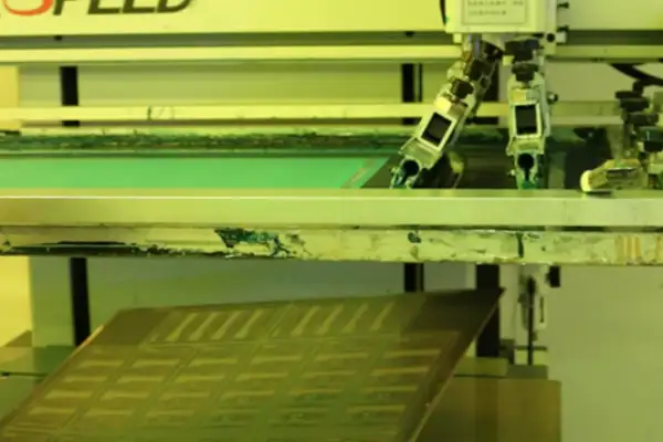
Even more troublesome is that HDI PCB manufacturing challenges are never a single-step problem. From lamination to drilling, each step adds uncertainty. For example, the core board’s expansion coefficient changes drastically after absorbing moisture, or uneven resin flow during lamination leads to voids. These microscopic defects might be tolerable on ordinary boards, but in high-density designs, they become fatal flaws. Actually, I think the industry needs to break free from the mindset that “the more precise, the better.” Sometimes, appropriately relaxing tolerances can lead to more stable output. After all, customers want reliable products, not just theoretical technical specifications.
Having worked on HDI boards for years, I’ve found that the most troublesome aspect isn’t the complexity of the design, but rather the invisible, subtle changes during the lamination process. Sometimes, even following standard procedures, unexpected deviations still occur in the finished product.
I remember once making an eight-layer board. After the first two laminations, the dimensions were within acceptable limits. However, after the third lamination, we found subtle interlayer misalignment at the edges. This deviation didn’t appear suddenly; it accumulated from the tiny differences in thermal expansion of the materials during each lamination. It’s like assembling building blocks; if each block is slightly off-center, the entire structure will eventually deviate from the center.
Temperature control during lamination is particularly critical. Once, to meet a deadline, we slightly increased the press temperature, resulting in localized warping of the board. We later discovered it was due to a mismatch in the thermal expansion coefficients of the different materials. Although the temperature difference was only a few degrees, it was enough to cause stress deformation in the inner core layer.
The most troublesome thing is that these deviations often only become apparent during final testing. Once, during impedance testing, we discovered significant fluctuations in values across different areas of the same board. Upon disassembly, we found that this was due to uneven dielectric thickness. It turned out that the flow state of the prepreg varied slightly with each lamination process, and these differences accumulated, causing the dielectric layer’s uniformity to become uncontrollable.
Now, we intentionally allow longer cooling time after each lamination to allow the material to fully release stress. Although the production cycle has lengthened, the yield rate has actually increased. Sometimes, going slower leads to greater stability—this is probably the unique characteristic of manufacturing high-density circuit boards.
In fact, making HDI boards is like battling various unseen forces. Temperature, pressure, and time—each factor is subtly at work, and all we can do is find that delicate balance point through experience.
Over the years of making HDI boards, I’ve increasingly felt that this work is like playing with a precision jigsaw puzzle—except each piece has its own quirks. This is especially true when dealing with multi-layered structures.
Take resin, for example; sometimes it’s truly a headache. Once, when we were making eight-layer boards, the resin in the middle layer flowed extremely unevenly. It wouldn’t flow wherever we wanted—at higher temperatures, it would spread everywhere; at lower temperatures, it resembled stale glue, leaving behind large and small air bubbles. The most troublesome part was between the intricate lines; if the resin wasn’t fully filled, debris would get stuck during subsequent drilling, a complete disaster. Later, we tried different viscosities of the formulation and discovered that the resin’s flowability had to match the board’s coefficient of thermal expansion.
Speaking of lamination, this step is even more demanding on patience. I’ve seen too many boards warp like potato chips due to improperly controlled lamination temperatures, especially when the core board thickness was inconsistent.
Actually, what struck me most about HDI was that even when every step followed the standard procedure, unexpected problems could still arise in the final product. Once, a batch of boards passed all parameters, but the impedance test kept fluctuating. It took three days of investigation to discover that the temperature and humidity fluctuations in the workshop were too large, causing different levels of moisture absorption in the boards.
Now, before starting any new project…
These experiences have taught me a valuable lesson: HDI manufacturing is never something you can master by simply copying textbooks. You have to be like a seasoned traditional Chinese medicine practitioner taking a pulse, constantly adjusting the process based on the characteristics of each batch of materials. Sometimes, the solution lies hidden in the most basic aspects—such as the storage environment of raw materials.
Recently, we’ve been trying a new method for lamination timing control.
Ultimately, the most fascinating aspect of this work is that you’re always dealing with the inherent characteristics of the materials themselves.
Over the years of working on HDI circuit boards, I’ve come to realize that the most troublesome thing isn’t the complexity of the design, but the hidden problems. Once, a board we made for medical equipment passed all routine tests, but after six months, the customer reported occasional signal interruptions. Upon disassembly, we discovered that the plating inside the micro-vias had developed minute fractures due to temperature changes—a problem that ordinary electrical testing simply cannot detect.
Now, the biggest challenge in HDI manufacturing is how to detect these “latent” defects in advance. For example, after the board has been exposed to high temperatures, the impedance in certain areas may subtly drift, but routine tests may show everything as normal. We later introduced a more refined impedance mapping technique to capture this dynamic change.
Speaking of inspection, I think we shouldn’t rely too much on a single method. X-rays can show internal structures, but they have limitations in judging plating thickness. We’ve learned this the hard way: a batch of boards had micropores that looked perfect on X-rays, but the actual plating uniformity was insufficient, leading to severe high-frequency signal attenuation. Later, we combined thermal cycling pre-aging with impedance measurement to truly control quality.
In fact, many HDI problems stem from a “good enough” mentality. For example, a 0.05mm alignment deviation might seem acceptable for visual inspection, but this small deviation can cause stress concentration in multilayer boards under vibration. We now prefer to set our inspection standards even stricter than customer requirements because the cost of rework is too high.
Recently, we’ve been trying a new inspection approach—focusing not only on static parameters but also on the board’s performance under simulated real-world operating conditions. For example, applying signals of different frequencies to the board while monitoring temperature rise often reveals hidden problems missed by traditional methods. This dynamic testing, although time-consuming, has indeed helped us avoid several potential quality incidents.
Ultimately, HDI manufacturing, like precision instrument manufacturing, requires more than just standard procedures; it demands a critical eye and meticulous attention to every step. Sometimes, the most inconspicuous detail can be the source of future problems.
My biggest takeaway from years of experience manufacturing HDI boards is that people tend to focus on visible metrics like linewidth and spacing. However, the true test of a factory’s skill often lies in those seemingly insignificant details.
For example, the solder mask process is particularly interesting. Once, we had a board requiring a 0.25mm BGA pitch design. When the client repeatedly confirmed the solder mask opening dimensions with the design, I initially thought it was an overreaction. However, the first batch of samples returned with several instances of short circuits caused by solder balls.
After careful analysis, we discovered the problem stemmed from the ink thickness. The factory, prioritizing efficiency, had made the ink layer too thin. While the alignment accuracy met, the high temperatures during reflow soldering caused slight ink shrinkage, exposing copper surfaces that shouldn’t have been exposed.
This incident made me realize that every step in HDI manufacturing requires an art of balance. Like walking a tightrope, too thick or too thin a layer will cause problems.
Speaking of soldering, I’ve encountered even more challenging situations. Once, when manufacturing motherboards for medical equipment, a nickel-gold plating treatment was required on pads with a 0.3mm pitch. During testing, black spots appeared in some areas.
This problem is particularly subtle because it’s not visually apparent; it’s only discovered during soldering due to a wettability issue. We eventually resolved the problem by adjusting the solution concentration and soaking time.
Now, whenever I review a new project, I pay special attention to the choice of surface treatment process. Different applications require different solutions; standard procedures cannot be simply applied.
In fact, the challenges of HDI manufacturing often lie hidden in these details. Sometimes, a seemingly minor parameter deviation can lead to the scrapping of an entire batch of products. Working in this industry for a long time has made me increasingly cautious because I know that every step is interconnected.
One interesting realization I’ve had over the years working on HDI boards is that sometimes the more advanced the technology, the easier it is to get bogged down in minutiae. The industry is always discussing controlling microvias to a fraction of a millimeter or achieving linewidths of a few micrometers, as if smaller numbers equate to superior performance. However, in reality, the common situation on production lines is that even if the parameters meet the standards, the yield rate remains low.
Once, we received an order for a smartwatch. The customer specifically requested 0.1mm laser drilling. During trial production, we discovered a strange phenomenon: the hole diameter accuracy was perfectly acceptable, but the signal transmission was unstable. We later found that fluctuations in the dielectric layer thickness caused impedance matching problems. This made me realize that in HDI manufacturing, perfection in a single step doesn’t guarantee overall performance.
Many engineers today easily get caught up in a parameter race, neglecting the interplay between different processes. For example, blindly pursuing smaller line spacing can lead to etching solution residue becoming a fatal flaw; excessively compressing the dielectric thickness can increase the risk of interlayer short circuits. These hidden challenges often test manufacturing skills more than the technical specifications in the tender documents.
The most successful case I’ve seen is actually a conservative approach—a medical device manufacturer insisted on using a slightly thicker dielectric layer. Although the theoretical wiring density decreased by 15%, the mass production yield remained stable at over 98%. Their product director made a very practical statement: “Instead of pursuing extreme data in the lab, it’s better to maintain a stable rhythm on the production line.” This pragmatic attitude is particularly helpful in dealing with real manufacturing challenges.
A recent automotive electronics project gave me a deeper insight. The client initially requested an arbitrary layer interconnect design, but we suggested a 2+N+2 structure. Although theoretical performance was slightly sacrificed, it avoided the deformation risk associated with five lamination processes. In fact, many high-end applications don’t require flashy technology stacking; the key is finding the most suitable technology combination for mass production.
Ultimately, when facing the various challenges of HDI manufacturing, perhaps we should focus less on the microscopic dimensions and more on the synergy of the entire production chain. After all, even the most sophisticated circuits must ultimately become reliable products—that will never change.
Through years of experience making HDI boards, I’ve gained some insights—many people ask… The problem is being overcomplicated. I once saw an engineer worrying about three months of data fluctuations in a CAF test report. This kind of failure is more like a test of our patience. The real challenge isn’t the technical parameters, but getting the young people on the production line to understand why they need to spend those extra ten minutes in the temperature-controlled workshop.
I remember a medical device project where the client insisted we disassemble and analyze a slightly dark solder joint. It turned out to be a capillary crack, barely noticeable even under a microscope. Later, we simply moved the potting process forward two steps; although the cost increased, similar problems never occurred again.
Now, everyone in the industry loves to talk about material certifications, but mountains of certificates are no match for a veteran production line worker’s touch. Last time, we tried a new material that claimed to have top-tier CAF resistance… The material’s performance was even worse than the standard model under conditions of sudden humidity changes. Sometimes data can be misleading, but the solder joints on the board won’t.
What surprised me most was that many large manufacturers treat the through-hole design as a prized possession. They insist on obsessing over micro-vias when a simple addition of a heat dissipation via would suffice. Once, dissecting a faulty board revealed that the expansion difference between the filler and copper caused the solder to crumble like a sour biscuit.
Actually, the worst thing in this industry is blindly chasing new trends. I’ve seen too many teams take foreign standards, change a couple of parameters, and call it innovation, only to fail to maintain even the basic through-hole yield in mass production. Good design should be like simmering soup over a low flame—you know when to reduce the heat, not constantly changing the pot.
Recently, a car electronics project has impressed me quite a bit. The client initially insisted on achieving the industry’s absolute limit on pitch, but later discovered that adjusting the wiring angle by 15 degrees was more effective than compressing the pitch. This is perhaps the challenge of HDI manufacturing—you have to find a reassuring balance beyond the specifications.
I’ve seen many people overcomplicate HDI board discussions. Actually, after working in this industry for a while, you’ll find that the most troublesome things are often the seemingly basic ones. Take the simplest example: sometimes, no matter how perfect your drawings are, the actual finished product just falls short.
Last week, our factory received an order from a client who insisted on ultra-fine pitch, and problems arose during the etching process. Even though we used the same batch of boards, the line width was… It’s almost two micrometers off. This kind of non-uniformity might not be noticeable on ordinary boards, but it’s a fatal problem in high-density designs.
Do you know what’s most infuriating? Sometimes the problem isn’t how advanced the equipment is, but the flatness of the substrate itself. I once specifically supervised a production line and found that even a slight waviness in the copper-clad laminate rendered subsequent exposures ineffective. Those tiny bumps and unevenness cause uneven photoresist thickness, directly affecting the verticality of the etching.
Now, the industry is full of hype about how amazing laser direct-write technology is, but what truly limits accuracy is often the stability of these fundamental processes. I’ve seen people spend a fortune on the latest LDI equipment, only to find that the yield rate was actually lower because the substrate wasn’t properly prepared in the preceding processes. It’s even cheaper than manufacturers using traditional equipment.
Ultimately, making high-density PCBs is like building with blocks. If the bottom layer is slightly crooked, no matter how many new technologies you pile on top, it’s all for naught. Especially when it comes to multilayer boards, if the inner layer lines aren’t controlled properly, even the most expensive equipment can’t salvage the outer layers.
Sometimes I feel this industry chases too many new terms and neglects the fundamentals. For example, the concentration control of etching solutions—old topics that few people are willing to discuss in depth now—yet these traditional processes determine the final success or failure.
I remember once visiting a long-established Japanese PCB factory; their temperature and humidity control in the workshop was outrageously strict, even regulating the frequency of employee entry and exit. At the time, I thought it was excessive, but now I realize it was indeed necessary. The reaction speed of copper foil during etching is extremely sensitive to environmental changes; a temperature difference of just two degrees Celsius can result in visible errors in linewidth.
Customers are now demanding increasingly higher linewidths, but the laws of physics remain unchanged. Instead of blindly pursuing parameter breakthroughs, it’s better to first ensure the stability of each step.
Having worked on HDI boards for many years, I’ve learned that sometimes the most difficult part isn’t meeting technical specifications, but rather the unseen stresses working in the shadows. Once, we were making a ten-layer board with a thin dielectric layer sandwiched in the middle. During testing, we discovered an abnormal signal; upon disassembly, we found that the inner copper traces were peeling up from the dielectric like tree roots.
This kind of problem is often not caused by a single step. For example, during the lamination process, high-pressure… High temperature and pressure cause a struggle between the copper and dielectric materials; one tries to expand while the other contracts repeatedly. After several such cycles, the bonding surface becomes exhausted. The most extreme example I’ve seen is a board that underwent six laminations, where the innermost copper layer detached with the slightest touch, as if thermal stress had worn away all its patience.
Thin dielectric layers are inherently contradictory. To control impedance, they need to be thin, but thinness means compromised mechanical strength. Once, a customer requested dense vias on a 2mil dielectric layer. The board developed micro-short circuits under slight pressure on the test fixture. It was later discovered that the dielectric layer had collapsed, causing adjacent signal layers to almost touch.
The problem with the conductive anode wire is even more insidious. A batch of boards passed all factory tests, but after being stored in a humid environment for three months, they suddenly short-circuited. Dissection revealed gaps in the fiberglass cloth. Thin copper wires, like vines, crawled out of the gap and connected to adjacent vias. This kind of problem is difficult to simulate during the design phase because it involves multiple factors such as material compatibility, humidity, temperature, and electric field distribution.
Now, when dealing with multilayer board projects, I pay more attention to material matching rather than just the stacking structure. For example, different types of fiberglass cloth in high-frequency boards have three times the resistance to capillary action (CAF). Sometimes, I’d rather adjust impedance calculations to avoid certain dielectric materials that are prone to capillary action. After all, the real challenge is the long-term reliability hidden behind the specifications, which is crucial for the board to be used in real-world environments for many years.
I’ve seen too many engineers idealize HDI during the design phase. They always think that simply maximizing the linewidth will solve the problem. The problem is that when you actually step into the workshop, you’ll find that those micron-level parameters are a completely different story in mass production.
Take core boards, for example. The ultra-thin materials achievable in the lab become as fragile as paper once they’re on a high-speed etching line. I once visited a factory that claimed to be able to do arbitrary layer interconnects and saw that they had specifically modified their conveyor system to handle 0.1mm core boards, reducing the speed to one-third of normal.
Many people pursue finer linewidths but ignore the actual limitations of the manufacturing process. I remember a customer insisting on 2-micron lines, resulting in the entire batch of boards being scrapped during electroplating due to uneven current density.
The real challenges often arise in unexpected places, such as multilayer board lamination. The issue of matching thermal expansion coefficients is crucial. Even a difference of a few ten-thousandths in the shrinkage rate of different materials can cause misalignment of microvias.
Some manufacturers are now using semi-additive methods for fine-grained circuitry, which is indeed more controllable than traditional etching, but the cost also increases. The key is to choose the process based on product positioning; it’s unnecessary to pursue the most advanced specifications for every board.
I admire factories that can achieve the ultimate in conventional HDI. They invest heavily in material pretreatment, such as special baking of the core board to reduce water absorption, thus preventing delamination during lamination.
As for arbitrary-layer technology, I think it’s currently more suitable for scenarios that truly require extremely precise wiring, such as certain high-end processor peripherals. If it’s just for basic functional expansion… There’s really no need to force such a high density in the design.
Sometimes simplifying the design can actually achieve better reliability. Using fewer layers of blind and buried vias and employing a more mature stack-up structure, while it may not look as cool, will significantly increase mass production yield, which is especially important for cost control.
In fact, you can judge a manufacturer’s skill level by how they handle seemingly simple steps. For example, a well-done inner layer black anodizing process can significantly improve the bonding strength of multilayer boards. Many large manufacturers have their own proprietary techniques for this.
In the future, we may see more applications of composite materials, such as mixing traditional FR4 with high-frequency materials. This has already begun in some specialized fields; although it’s more difficult to process, it can simultaneously meet electrical performance and mechanical strength requirements.
Over the past year, I’ve noticed an interesting phenomenon—many people believe that smaller apertures are always better when it comes to high-density interconnects. But that’s not actually the case. I’ve seen many design drawings densely packed with 0.1mm laser-drilled holes, which looks impressive, but often overlooks fundamental issues like heat dissipation and stress.
I remember last year a customer brought us an eight-layer PCB, saying that small batches they’d done at another factory kept having problems during testing. When I looked at the drawings, I laughed—the entire board looked like fabric riddled with needle holes, with blind vias surrounding critical signal lines. This design might be perfect in theoretical calculations, but in actual production, the heat-affected zones from laser drilling will overlap, causing localized embrittlement of the dielectric layer. Later, we suggested he increase the aperture in non-critical areas to 0.15mm. Although the density appeared to decrease, the yield actually increased from 60% to 85%.
There’s a misconception in the industry now that more laminations equate to higher quality. Once, during a design review, I saw a six-lamination design and immediately asked the engineer: “Are you sending this board into space or something? Ordinary consumer electronics don’t need such a complex structure; three laminations are sufficient for 90% of needs.” Each additional lamination introduces new risks of alignment deviations, and the repeated exposure to high temperature and pressure causes significant fluctuations in resin flow and dielectric layer thickness.
Speaking of materials, I’ve recently come to realize… This is an underestimated aspect. Even with the same polyimide substrate, the moisture absorption rate can vary by more than two times between different manufacturers. Last month, during our accelerated aging tests, we found that a cheaper material developed microcracks after only 200 hours in a humid and hot environment, while better materials held up to 500 hours with the solder pad interface intact. This reminded me of a lesson I learned years ago—a batch of boards, after being stored at the client’s location for six months, began to crack, and it was eventually discovered that a mismatch in the core material’s TG value caused an excessive Z-axis expansion coefficient.
Actually, the most dangerous thing in this industry isn’t technical difficulties, but the mindset of blindly pursuing parameter specifications. At the last exhibition, I met a young engineer who excitedly told me they had broken through the 3/3 mil linewidth and spacing limit. I countered with a question: “Do you know what this means for etching solution control? When the copper foil thickness deviation reaches 20%, the current carrying capacity of fine lines drops by 40%. Instead of getting bogged down in these numbers, it’s better to focus on optimizing the grounding layer distribution.”
I’ve recently been working on an automotive electronics project. The client initially insisted on a 0.08mm microvia design. We showed him simulation data: under cyclic impact with a 100-degree temperature difference, the probability of hole wall cracking with this aperture size is three times that of a 0.15mm aperture. We later changed to a hybrid via design—fine vias for critical signal areas and standard vias for power supplies, ensuring both performance and improved reliability. This flexible approach is key to handling HDI… The key challenges of PCB manufacturing.
Sometimes, looking at the precision equipment in the lab, I think, “Laser drilling machines can now achieve repeatability of ±5 micrometers, but what truly determines the quality of the board is the control of some basic processes.” For example, in the pre-plating descaling process, many factories simplify the process to save time, resulting in the hidden danger of resin residue. There’s an old photo on our workshop wall—a master craftsman inspecting the hole walls with a magnifying glass; fewer and fewer people are willing to do this kind of painstaking work now.
Ultimately, HDI PCB manufacturing is like building with blocks. It’s not about how exquisite each individual block is; the key is the balance of the overall structure. I’ve seen too many cases of pursuing extreme parameters and ultimately failing. On the contrary, designs that leave sufficient safety margins are the ones that stand the test of time. Next time you’re preparing to stack more blind and buried vias, ask yourself first: Is it really necessary to be so extreme?
My deepest realization from years of working with HDI boards is that the real test of skill is often not the high-end equipment parameters, but the ability to handle details. I remember once processing an eight-layer arbitrary-layer board where the laser drilling precision was clearly up to standard, but… We stumbled during the electroplating process. It turned out that a two-second delay in the plasma cleaning time during the hole wall pretreatment resulted in residual trace carbides, causing insufficient copper layer adhesion and leading to delamination during thermal shock testing.
In fact, this kind of invisible killer is the biggest fear for high-density interconnect boards. You think drilling a hole diameter of 0.1mm is enough? The real challenge lies in ensuring uniform copper ion deposition within such fine micropores. For a while, our lab spent all our time studying the flow patterns of the electroplating solution under different aspect ratios. We later discovered that simply adjusting the current density wasn’t enough; we also had to consider the effect of the solution’s surface tension on bubbles at the bottom of the holes.
Speaking of HDI PCB manufacturing… Many people’s first thought about challenges is interlayer alignment, but the electroplating process itself has even greater variables. For example, even with the same specifications of board material, the moisture absorption rate of the hole walls can differ by up to three percentage points in high humidity during summer, directly affecting the copper plating activation effect. Once, during mass production, voids suddenly appeared inside the holes; a review of the process records revealed that the chemical bath concentration drift was caused by temperature fluctuations in the constant temperature chamber.
Currently, the industry loves to boast about the micron-level precision of laser drilling, but few mention the crucial role of subsequent processing. Just like in home renovation, no matter how beautiful the grooves are, if the wall base isn’t properly prepared, cracks will inevitably appear later. After learning from our mistakes, we conducted a comparative experiment and found that under the same conditions, extending the ultrasonic cleaning time can optimize the hole wall roughness by more than 30%, which is a qualitative leap in improving the adhesion of the subsequent copper layer.
Recent cases involving medical devices have further convinced me that the real barrier to HDI manufacturing lies in the stability of the entire process. One client required the micro-hole plating thickness tolerance to be controlled within ±5%. We tried seven different additive formulations and finally achieved the target using reverse pulse electroplating. Clients never seem to care about these details, but they are often the key to the success or failure of a project. Key.
Sometimes I feel that making high-density PCBs is like micro-sculpture; every step requires meticulous attention to detail, like wearing a microscope. After all, when the wire spacing is as small as tens of micrometers, any seemingly insignificant deviation is magnified geometrically. Working in this industry for a long time actually cultivates a respect for traditional processes—at least they allow for much greater tolerance for error.
In my years of working on HDI boards, I’ve noticed a rather interesting phenomenon—many people think the most difficult parts are the visible technical specifications, such as line width and spacing, but what truly torments us are often the aspects hidden within the manufacturing process. Details such as the alignment accuracy during multilayer board lamination are crucial. Even if the first few layers are perfect, a cumulative error of a few tenths of a millimeter during the fifth or sixth lamination can ruin the entire batch of boards. It’s like building blocks; the higher you go, the more likely they are to wobble.
I’ve seen many factories initially focus solely on adjusting electroplating parameters, tossing and turning duty cycles and reverse pulses for ages, only to get stuck on lamination alignment. While electroplating filling is indeed crucial, especially when dealing with micro-pores like 0.1mm, even slightly poor solvent flow can leave voids. However, the hidden dangers caused by interlayer misalignment during multilayer lamination are far more insidious—they don’t immediately surface; they might only be discovered during customer component placement, at which point assigning blame becomes extremely difficult.
Speaking of electroplating, I don’t think it’s necessary to excessively pursue theoretical uniformity. Some manufacturers insist on controlling the copper thickness difference on the board surface to within ±3μm. In reality, for most consumer electronics products, ±5μm is already reliable enough. Overly pursuing perfection can easily make the plating solution fragile; even slight fluctuations in incoming materials require adjustments to the entire plating solution. We previously tried a more pragmatic approach—appropriately relaxing the recess depth requirements during the via filling stage, focusing our efforts on ensuring the adhesion of the copper layer. After all, users are more concerned about whether the board will delaminate after two years, rather than whether the surface flatness can be measured to three decimal places.
Another small detail is that many people easily… While neglecting temperature shock testing can indeed reflect reliability, in real-world applications, boards are mostly exposed to gently rising temperatures over long periods. For example, mobile phone motherboards typically operate at around 40-50 degrees Celsius. Extreme situations like a sudden jump from -50 degrees Celsius to over 100 degrees Celsius are extremely rare, occurring only once in a decade. Instead of obsessing over increasing thermal cycling lifespan by three to five times, it’s more important to focus on the stability of materials under long-term moderate temperatures, especially the dielectric constant drift of high-frequency boards with temperature – that’s the real pain point affecting signal integrity.
Looking back, the difficulty of HDI manufacturing has long since shifted from single-point process breakthroughs to a global balance art. When adjusting electroplating parameters, you have to consider not hindering lamination; when selecting fillers and resins, you have to consider not affecting the efficiency of subsequent laser drilling. These steps are interconnected; sometimes, a slower pace is actually faster.
Many engineers focus too much on technical parameters early on and overlook
As someone who has worked in PCB outsourcing for years, I’ve found
Cramming a camera, amplifier, dual-mic array, and Wi-Fi radio into a palm-sized
- خبير في إنتاج دفعات صغيرة إلى متوسطة الحجم
- تصنيع ثنائي الفينيل متعدد الكلور عالي الدقة والتجميع الآلي
- شريك موثوق لمشاريع تصنيع المعدات الأصلية/التصنيع عند الطلب الإلكتروني
ساعات العمل: (من الإثنين إلى السبت) من الساعة 9:00 إلى الساعة 18:30
Get quote, solution or any question, Andre always here to help