

Why the Best PCB Supply Chains Are Built Like Relationships, Not Transactions: Lessons for Satellite Communication PCB Programs
What actually makes a long-term PCB supply chain partnership work — shared
The visible headline in GPU expansion card design is usually the chip. Transistor count, memory bandwidth, compute performance in benchmark titles — these dominate product coverage. But engineers who build systems around high-end GPU cards know that the chip’s rated capability is a ceiling, not a guarantee. Whether the card reaches that ceiling depends substantially on the PCB carrying it.
Personally assembling a workstation for local AI inference and discovering that a current-generation card cannot sustain full performance on an older motherboard is a useful calibration. The bottleneck is the interface — specifically, the PCB that connects the GPU to the rest of the system and determines how cleanly power is delivered and how faithfully signals are transmitted.
The Physical Constraint of High-Layer PCB Manufacturing
GPU expansion cards for high-end compute applications use PCBs with layer counts that are challenging by any manufacturing standard. Twenty layers or more is common for cards with dense BGA components and multiple DDR memory packages. Some designs push significantly higher. Each layer represents a controlled processing step; errors accumulate across steps.
Lamination registration is the critical discipline at high layer counts. Each set of inner layers must align precisely with every other set before the final lamination cycle. Registration error in any layer creates misalignment between via landing pads and the conductors they are intended to connect. At normal layer counts, accumulated registration error is typically manageable. Beyond fifteen or twenty layers, it becomes the dominant variable affecting yield.
The challenge is compounded by thermal expansion during lamination. Every material in the stackup expands during the press cycle at a rate determined by its individual coefficient of thermal expansion. Where those coefficients are not identical — which is the case in any mixed-material stackup — differential expansion during heating and differential contraction during cooling introduce relative displacement between layers. Sophisticated lamination presses with multiple independent temperature zones can manage this by controlling local heating rates. But the process window narrows as complexity increases.
For designs using multiple substrate materials — different dielectrics optimized for different performance requirements in different functional regions — the interface between material types becomes a specific reliability concern. Resin systems with different chemistries may not form strong bonds at their interface under high-temperature lamination conditions. This produces delamination risk that appears initially as a processing defect and, if not caught, as a field reliability failure. The project case where a seven-material stackup produced first-article yield below thirty percent — and required eight months of process development to stabilize — illustrates the difficulty. Each material interface required characterization of flow behavior, gel time, adhesion promotion requirements, and thermal expansion matching.
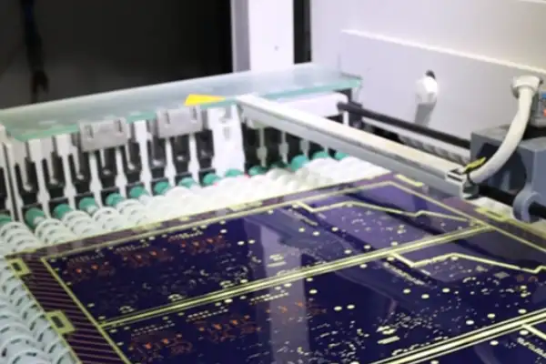
Power Delivery: The Overlooked Determinant of GPU Performance
Power delivery network design receives less discussion than signal routing in GPU card development, but its quality directly limits compute performance. A high-performance GPU operating at full load draws current that can vary by hundreds of amperes between low-power and full-compute states. The voltage regulator must supply this current while maintaining the core voltage within a few percent of its nominal value. Every milliohm of resistance and every nanohenry of inductance in the path between the regulator output and the GPU core degrades its ability to do this.
The PCB contributes to this impedance through the resistance of its copper planes, the inductance of the current path, and the effectiveness of the decoupling capacitor network. Thick copper in the power planes reduces resistance. Short, direct current paths reduce inductance. Decoupling capacitors placed immediately adjacent to the GPU’s supply pins — not remotely distributed across the board — provide the local charge reservoir that sustains voltage during rapid demand changes.
Heavy copper processing is relevant here: the lower resistance of thicker copper directly reduces the voltage drop that occurs when large currents flow during peak compute operations. The same copper thickness that improves power delivery also helps spread heat away from the GPU package, since the power and thermal conduction functions share the same conductor geometry.
The BGA mounting of high-performance GPUs adds a requirement for PCB flatness that interacts with copper thickness selection. Very thick copper in inner layers creates mechanical stiffness variation across the board area. If the stiffness is not symmetric about the board’s midplane, warpage occurs at the soldering temperature during assembly. Warped boards produce non-uniform BGA joint formation. Some joints receive inadequate solder volume; others receive too much. Both conditions reduce reliability. The solution is not simply choosing a different copper weight but designing the stackup so that copper distribution is symmetric about the neutral axis of the structure — a requirement that sometimes conflicts with performance-optimized routing plans.
Via Aspect Ratios and Plating Quality
The density of high-end GPU expansion cards requires vias with high aspect ratios: the via depth divided by the via diameter exceeds six or eight in many designs. Electroplating these structures uniformly is a process challenge. Plating solution must flow into the via and deposit copper on its walls at a consistent rate from top to bottom. As aspect ratio increases, this becomes increasingly difficult. The interior of the via sees less fresh plating solution than the entrance, reducing deposition rate. The result is thinner plating at the mid-depth of the via than at the surface.
Thin plating in the barrel reduces the via’s current-carrying capacity and increases its resistance. Under thermal cycling — which occurs every time a GPU card is powered on and off — the via undergoes dimensional change as the surrounding material expands and contracts. Thin plating has less structural reserve to accommodate this cycling before fatigue cracking develops. The crack may not be visible and may not immediately affect electrical continuity, but it will propagate under continued thermal stress.
Pulse plating addresses this by improving solution distribution into the via interior, reducing the deposition rate differential between surface and interior. But the effectiveness of pulse plating depends on specific bath chemistry, current waveform parameters, and the ability to maintain consistent process conditions across a production run. A supplier who claims pulse plating capability but cannot describe how they verify bath parameter stability and deposition uniformity across panel positions is not demonstrating process maturity.
Back-drilling the stubs from high-speed through vias on GPU expansion cards addresses signal integrity but creates its own precision requirement. The drill must reach a specific depth to remove the unused stub while not penetrating the last active via connection. Depth control at plus or minus 0.05 mm is achievable with well-maintained equipment and disciplined process control; less precise back-drilling produces inconsistent stub lengths that partially defeat the purpose of the operation.
Evaluating Multilayer PCB Suppliers for GPU Applications
The questions that reveal genuine capability are more specific than “can you build this layer count.” They probe process understanding and process control depth.
For lamination: How do you compensate for interlayer registration error that accumulates across high layer count stackups? What temperature zone configuration do you use for this specific material combination, and what is the basis for that selection? How do you verify registration quality during production rather than only in first-article inspection?
For plating: What is your characterization of via barrel plating uniformity as a function of aspect ratio? How do you monitor plating bath condition and what is your response to drift? Can you provide cross-section data showing plating distribution across a range of via depths from representative production panels?
For materials: Have you previously processed this material combination? What interface adhesion testing have you done at the boundaries between different dielectric systems? What failure modes have you observed, and what process adjustments resulted?
Suppliers whose engineering team can engage with these questions using specific production data are demonstrating the depth of process knowledge that high-layer-count GPU board manufacturing requires. Suppliers who respond with general capability assertions are representing their equipment, not their process.
Liquid Cooling Integration Changes the Design Problem
The increasing adoption of liquid cooling in high-performance compute applications creates an opportunity to revisit fundamental assumptions about how GPU expansion cards are designed. When heat removal is managed by direct liquid cooling at the component level, the thermal constraint that previously drove many PCB design decisions — how to move heat away from the GPU package through the board — changes character.
This opens the possibility of organizing high-power components around the cooling structure rather than around thermal spreading considerations. Power delivery paths can be shorter and more direct. The board’s role shifts toward providing the highest-quality electrical interface possible rather than serving as a thermal management intermediary.
But liquid cooling integration introduces its own PCB compatibility requirements. Coolant distribution manifolds interact mechanically with the board surface. Sealing requirements affect which board regions can accommodate thermal interface materials and mounting hardware. Some coolant chemistries affect specific substrate materials or surface finishes over long exposure durations. These are engineering problems that require the PCB design and the liquid cooling system design to be developed together, with manufacturing input from a supplier who understands both sets of constraints.
The systems thinking that produces reliable GPU expansion cards is not confined to any single design parameter. It encompasses signal integrity, power delivery, thermal management, mechanical reliability, and manufacturing feasibility simultaneously. Layer count is a result of correctly balancing these requirements, not a starting specification. The boards that enable consistent GPU performance across demanding applications are built by engineers and manufacturing partners who approach the design problem that way.
What actually makes a long-term PCB supply chain partnership work — shared
Practical, experience-based strategies for how to reduce PCB procurement risks — from
Real factory-floor lessons on how to optimize a PCB manufacturing process —
- خبير في إنتاج دفعات صغيرة إلى متوسطة الحجم
- تصنيع ثنائي الفينيل متعدد الكلور عالي الدقة والتجميع الآلي
- شريك موثوق لمشاريع تصنيع المعدات الأصلية/التصنيع عند الطلب الإلكتروني
ساعات العمل: (من الإثنين إلى السبت) من الساعة 9:00 إلى الساعة 18:30
Get quote, solution or any question, Andre always here to help