

Automotive Rain Sensor PCB: How Optical Paths, Potting, and Fabrication Quality Decide Field Performance
Do you think a rain sensor is just a simple circuit board?
When running a 5G base station, everyone stares at the antenna and the RRU, but the PCB underneath that handles fiber backhaul is actually where the most skill is needed. In a project I handled not long ago, things went wrong exactly on the Fiber Backhaul PCB. The samples delivered by the board factory made the 100G optical module drop packets wildly as soon as it was powered on, and when I hit it with an oscilloscope, I found the stubs of the high-speed differential pairs had not been cleaned up at all. This incident completely changed my approach to choosing a multilayer pcb manufacturer.
I used to be particularly superstitious about layer count, thinking that for a backhaul board, stacking twenty layers and using top-grade high frequency PCB material would settle everything. Later, after stepping in pits one after another, I understood it is not like that. Some multilayer pcb suppliers, to cut costs, have uneven inner layer copper thickness, with impedance jumping all over the middle of the board, and the eye diagram of a 25G NRZ signal is miserably unwatchable. Later I switched to an hdi pcb supplier that specialized in communication backplanes. They used an improved prepreg lamination process to hold the phase difference of differential lines in a very small range, and the waveform immediately became clean. This really has no direct relation with how advanced the equipment is. It is just a matter of how careful the work is.
5G backhaul and fronthaul demand entirely different things from the board. Backhaul runs long distances and optical modules consume a lot of power, so the copper on the board that supplies power must be able to carry high current, and if heat dissipation is handled carelessly, the area beside the optical module pads can be hot to the touch. So when I later looked for a high frequency PCB manufacturer, I would directly ask about their experience in mixing thick copper and high-frequency substrates. Many factories advertising themselves as a high frequency PCB supplier start to hedge on the quote as soon as they hear 3oz copper with M6-grade dielectric. The circle of those that can do this steadily is only so big.
Another type of baggage is HDI. Many people think a board made by an hdi pcb manufacturer is naturally suited to high-speed backhaul, but it is really not so. I tested a Fiber Backhaul PCB that used microvias, and reflection above 25G was outrageously large, not even as good as a traditional through-hole board. The reason was that the structure and position of the blind vias happened to sit right on the critical return path. A board, in the end, is decided at the layout stage by one’s understanding of signal return and isolation, and the factory only etches these understandings onto the substrate at the end.
As for boards for industrial optical networks and submarine optical cables, that is another kind of tinkering. In industrial environments, sulfide corrosion can gnaw an ordinary PCB until it looks unrecognizable, and it must also be compatible with ultra-low-latency SerDes routing. Every time I go around looking for a multilayer pcb supplier, those who can swallow all these extreme requirements together can be counted on one hand. So, in this business of 5G backhaul and optical networks, do not covet saving trouble. When choosing suppliers, ask a few more questions about actual details, which is more useful than looking at layer counts and advertising words.
In these years in the optical communication circle, my deepest feeling is that if the board is chosen badly, the later work is basically digging pits for yourself. Especially for backhaul, a Fiber Backhaul PCB is not at all the same thing as an ordinary digital board, and many newcomers still apply the switch-design thinking to it and flip over as soon as they go to high frequency.
I have a friend who makes base station fronthaul modules, and he took a big loss last year. To save trouble, he went to an hdi pcb manufacturer that had not done much with optical modules. When the board came back and was measured, the 25G signal’s eye diagram was as if closed, and after a long investigation he found the stackup was not handled well and differential impedance deviation was too large. This was only small-batch validation, and had it been mass production, the loss would have been more than a little. Later he switched to a multilayer pcb manufacturer specializing in high-speed multilayer boards. They started by asking which optical module he used, how high the rate was, how long the longest trace was in mils, and which process to choose for vias, and went through a pile of things he had not cared about before. After that I understood that for fiber backhaul boards, the experience of the vendor matters far more than equipment parameters.
Many people think finding a multilayer pcb supplier only requires looking at price and delivery time, which is a big mistake. What runs on the backhaul is not only high-speed SerDes but also high-current power supply and an analog optical receiving chain, and a slight carelessness in layout lets digital noise couple to the receiving end, and sensitivity drops directly by several dB. I have seen a board where the laser driver circuit was too close to the digital processing part and the thermal copper was not laid enough. After module temperature rose, wavelength drifted and errors soared, and in the end the only option was a revision. This kind of problem is the result of a disconnect between board factory process and design. When you take the drawing over, some factories just build as drawn and will not remind you what is unreasonable.
So when I select suppliers now, I always ask whether they have mass-produced boards with optical modules, especially 25G and 100G. For this kind of product, the capability of the hdi pcb supplier is very important, because very often, to compress the trace length between the module and main chip, you must use laser blind vias or an any-layer interconnect HDI structure, otherwise loss gets large and you can forget about signal integrity. HDI boards demand extremely high uniformity in lamination, drilling and plating, and not just any factory can hold it steady.
Another often-neglected point is board material. The Fiber Backhaul PCB runs 28Gbps or even higher, and ordinary FR4 dielectric loss simply cannot bear it, so high-frequency, high-speed board material must be used. I am rather superstitious about the original manufacturer’s recommendations for high-frequency materials. I have tried several high Frequency PCB manufacturers, and although some used materials with nominally good Dk and Df, the dielectric thickness tolerance after actual lamination was large, directly affecting phase consistency, which is deadly in clock-sensitive scenarios like CPRI or eCPRI. A high Frequency PCB supplier I cooperated with later was willing to test characteristic impedance both before and after lamination and to attach the measured data to the shipping report. Using that kind of factory is much more reassuring.
Ultimately, a PCB in this kind of fiber backhaul system is never a generic part. It is tightly bound to the optical module, protocol and thermal structure. If you change only one module model, the original board may not be directly reusable. My habit is that whenever a new module is to be integrated, I always pull in the board factory and the module vendor for a joint evaluation, going through power supply, heat dissipation, high-speed routing and isolation from scratch. Missing any link can bring surprises later.
For backhaul boards, slow really is fast. Spend more time in the early stage choosing the right factory and working details through, and there will be less rework. Otherwise, tuning the module while suspecting the board has problems is a torture that I hope you will never experience.
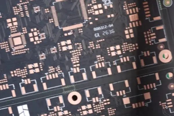
During the time I worked on fiber backhaul boards, I once thought the hardest part was signal simulation, and later found it was not. Finding an hdi pcb manufacturer that could stably handle mixed lamination was the real tour of pits. There is a very funny reality in 5G fronthaul: protocols evolve too fast, eCPRI had only landed for two years, and the engineering departments of many board factories were still stuck in the old CPRI calendar, thinking that 10G per lane was enough. When you mention 25G SerDes routing to them, their first reaction is to put you in the category of overclocking players.
At that time I was going around with a 20-layer board requirement, needing to mix high-speed material, with high-current power on the back as well. Quite a few multilayer pcb suppliers, hearing FR408HR mixed with Megtron 6, quoted a sky-high price directly, and some simply said they could not do it and recommended I reduce layer count and change the design. But this could not be compromised: with 25Gbps running on it, if the via stub from surface microstrip to inner stripline is left a bit longer, the eye diagram closes right in front of you. Later I drew a comparison table myself and screened the high Frequency PCB manufacturers of the Yangtze River Delta and the Pearl River Delta one by one. Some factories had very new equipment but did not understand why we insisted on back drilling controlled to plus or minus 2mil, and after the workers drilled, they saw 8mil of stub remaining and still felt it did not matter. Boards like that, when taken back and tested on the machine, had return loss exceeding the limit directly, a wasted effort.
I bit the bullet and switched to a smaller multilayer pcb manufacturer specializing in base station transmission boards, and the communication cost dropped immediately. Their CAM engineers had designed optical modules themselves and knew how much tighter the link budget became after CPRI moved to eCPRI. For our odd requirements, such as controlling intra-pair skew within 1ps, and doing so along an entire 6-inch trace, they ticked the box on the engineering confirmation sheet without needing an explanation. For the several groups of high-speed lines on the Fiber Backhaul PCB headed to the SFP28 cage, they proactively proposed handling the reference layer opening as a coplanar waveguide, saying tests showed crosstalk could be pressed down another 2dB, which was more solid than relying on spacing alone.
Later I understood that making this kind of board, finding the right multilayer pcb supplier is not about how long its certification list is. High-speed materials can be bought by anyone, and the key is whether those people are willing to tune lamination parameters separately for your design. A high Frequency PCB supplier left a deep impression on me. They had specially made test tables of how DK and DF change with frequency for mixed lamination structures. When sent over, the dispersion from a few GHz to over twenty GHz was more conservative than the original manufacturer’s datasheet but accurate to an unusual degree. Doing simulation with that kind of data gives you real confidence.
Right now 5G transport is not the end. Fronthaul bandwidth keeps expanding, 25G will soon be full, and people are quietly validating 56G PAM4 and even 112G beyond that. At this point, relying on an hdi pcb supplier that only copies public-version stackups really drags you down. My habit now is that for a new project, before drawing the schematic, I first confirm with the board factory whether they have made a Fiber Backhaul PCB of a similar rate, and look at their actual cross-section reports and loss test data. Those who can directly produce a mass-production case of a 100G SR4 optical module PCB can be sized up in two sentences, saving a pile of trial-and-error cost. The PCB in a high-speed link is never a passive carrier. It is itself a device.
What is feared most in a project? It is not that you cannot work out the signals, but being fooled by factories carrying the multilayer pcb manufacturer name. They dare to use ordinary board material to carry high-speed routing, and when prototypes come back, the eye diagram is fully closed and the whole board is directly scrapped. Now when handling a high-density board like the Fiber Backhaul PCB, I do not at all believe a supplier’s claim that it can do it, but look at whether they have continuously delivered module carrier boards of the same grade. Many so-called multilayer pcb suppliers cannot even control back drill stub depth steadily, and the via stubs they produce are like antennas, stirring the reflection resonance on the module side into a mess.
Do you think the job is finished once the PCB stackup is set? Far from it. This backplane is covered with optical module interfaces, space is extremely compressed, and ordinary routing methods cannot get lines out at all. Then you have to stack up the HDI structure, but a solid hdi pcb manufacturer is rarer than a giant panda. I met an hdi pcb supplier that used laser blind vias to connect those few critical signal layers, and the result was fractured hole copper, and the whole batch of boards simply dropped the ball in the vibration test, nearly ruining the entire delivery milestone.
After stepping in so many pits I understood: do not treat impedance control as a mere numerical game. The impedance test reports given by many of those multilayer pcb manufacturers are dead data in a static environment and do not consider the drift of dielectric constant after the board heats up. For a board like the Fiber Backhaul PCB running high-speed signals all over, I now only work with high Frequency PCB manufacturers who can provide wide-temperature dynamic impedance data. If the etching precision of the golden finger pad transitions of each module on this board is insufficient, the reflection it causes is more fatal than a long stretch of routing. Many high Frequency PCB suppliers, to save trouble, treat the pad as an ordinary pad and do no gradual optimization at all. Ultimately, a hardware person cannot hand their life to the process bottom line of others. When unsure, I would rather spend two more rounds of prototype fees than find an hdi pcb supplier who cannot swallow this meal and prop it up, leaving the whole PCB as an expensive piece of scrap.
I have always felt that the industry hypes board materials and stackups too much, and few people seriously talk about the landmines hit when choosing suppliers. Last year we had a 400G optical module project. At the beginning, to save trouble, we directly picked from our original multilayer pcb supplier list a factory that cooperated reasonably well, thinking it was just a Fiber Backhaul PCB with some more layers and finer lines, nothing big. The result was that when the first batch of boards came back, the SerDes channel eye diagrams were fully closed, errors at 25G ran all over the sky, and debugging the optical front end nearly made us doubt life.
Later I carefully checked the process report and found that the multilayer pcb manufacturer’s control of back drill depth fluctuated enormously, with remaining stub often exceeding 12mil, and copper thickness within the differential pair was uneven, causing a nominal 100 ohm impedance to float above 110 ohms across the board. You cannot simulate this in EDA software ten thousand times. It is purely a capability gap on the processing end. So we simply changed strategy and re-evaluated several hdi pcb suppliers with volume back drilling capability. The one we finally settled on was both an hdi pcb manufacturer and had its own high-frequency hybrid lamination line, which directly applied the process experience of a high Frequency PCB manufacturer to the digital module side. For example, they used laser drilling to control the etching precision of microstrip lines, and for the differential pin escape segment alone, skew was pressed down to under 1ps.
The module, which is the optical transceiver unit we commonly talk about, actually has its hardest part not in the optical path but in the dozen or so SerDes pairs of PCB routing from the golden finger to the DSP and then to the optical engine. If the supplier you find only builds as drawn and does not do layer registration compensation and dynamic residual copper rate adjustment, the board they make is basically unwatchable above 25G. So now when I choose a high Frequency PCB supplier, I do not look at the 56G/112G supported written on their PPT but at whether they can make the single-ended and differential TDR curves nearly overlap, and whether they can provide the impedance distribution chart for a whole batch of boards. A truly reliable hdi pcb manufacturer, when you give them the stackup file and design requirements, will back-calculate the time difference of the differential pins and then give recommendations on which drill to use, how large a bit, and how many deburring passes, rather than throwing you an engineering confirmation sheet to sign and be done.
In these years of working on high-speed SerDes, my personal biggest change is no longer treating the PCB as a passive part. It is itself a high-precision microwave component. Every differential pair and every via layer change is ground out bit by bit by the multilayer pcb manufacturer that tunes drill bits on the production line every day, and not accomplished by sticking an ideal model in simulation software. So now, for a new generation of 800G modules, I would rather spend a month in the early stage doing a DFM review with the hdi pcb supplier, picking apart copper foil roughness, glass fiber direction and the shape of solder mask openings one by one, than staring at an error rate tester worrying later.
Many people, as soon as optical module rates are mentioned going up, immediately look at board materials and process parameters, as if as long as they change to ultra-low-loss material and find a similar hdi pcb manufacturer to squeeze line width and spacing a little, the signal can run up stably. This idea itself is not wrong, but the losses I have suffered in real projects tell me that what is truly headache-inducing is often not these things written on spec sheets.
Two years ago I worked on a 400G module project. At selection time we compared several multilayer pcb suppliers, and the differential impedance in the test boards they all brought out, measured on a vector network analyzer, looked pretty good, with a nominal plus or minus 5% tolerance that looked sufficient any way you cut it. But when it came to actual panelized production, the problem arrived. For different batches of the same PCB, the insertion loss dispersion was outrageously large. After investigation we learned that the multilayer pcb manufacturer, to chase capacity, had slightly adjusted lamination parameters and had not controlled copper foil roughness, and as a result the modules we sent out had eye diagrams collapsing by half on the customer’s switch. This made me understand one thing: for the Fiber Backhaul PCB used by optical modules, what is competed is not who marks parameters more aggressively but who can fully master consistency.
Later we moved the board to a high Frequency PCB manufacturer specializing in high-frequency hybrid lamination. Cost indeed went up, but the TDR curves of every board could nearly be overlapped. After chatting more with their engineers, I found an interesting detail: when they make this kind of high-layer-count board, they do not treat impedance tolerance as a dead line to guard, but look instead at the drift of dielectric constant across the whole production batch. For high-speed signal routing above 50Gbps, with a temperature rise of a dozen degrees, the dielectric’s own er may change only a few tenths, but reflected in the link budget it is a loss difference of several dB. Many hdi pcb suppliers that only repeat the parameter table will not mention this to you.
There is another neglected point, which is the thermal path design of that small PCB in the optical module. Module power consumption rises year after year, the laser and DSP chip are squeezed into that little place, heat cannot get out, and optical power drops directly. I used to think that adding enough copper thickness or filling thermal vias was enough, and only after cooperating with an hdi pcb manufacturer that made high-density interconnect did I understand that the selection of thermal via plug material and the density of copper fill matter far more than the number of holes. They had a board using stepped copper-block embedding with thermal resistance nearly thirty percent lower than conventional design, and this structure demands extremely high layer-to-layer alignment in a multilayer board, which an ordinary HDI factory simply cannot handle. At that point you find that a truly reliable Fiber Backhaul PCB supplier must be one with unique understanding in process details, not one that only takes orders and schedules production.
There is a rather helpless trend in the industry now, which is that many people simplify high-speed PCB selection into three steps of choosing board material, choosing line width and choosing a manufacturer, as if throwing the task to a high Frequency PCB supplier settles everything. But once the rate passes 100Gbps and the signal modulation changes to PAM4, the noise tolerance is cut by a large chunk, and every section of copper conductor and every via stub in the link becomes an uncertainty. My habit is that in the early stage I regard myself as an assembler: holding the cross-section report given by the supplier, I use a microscope to look at the steepness of the copper foil sidewalls and whether prepreg filling has voids. This work is earthy but more real than any inspection report. After all, the module is finally stuffed into a switch and runs in a machine room for several years, and no one will exempt you from pits in your link budget because of a nice-looking sheet of data from a supplier.
Ultimately, in the field of the Fiber Backhaul PCB, technology iterates fast, but the pattern of stepping into pits has not changed in over a decade: the finished board you can get is always only a compromise between that factory’s engineering ability and its quality bottom line. Rather than fuss over a few tenths of a dB on the parameter table, it is better to spend time finding a multilayer pcb manufacturer willing to dig into process details with you. This is the most valuable shortcut in high-speed optical module hardware.
Earlier, in a backhaul network project, I nearly had a breakdown over the choice of PCB supplier. That project used a Fiber Backhaul PCB with a high signal rate, and the board material had to be low-loss, with several dielectrics mixed in lamination. The multilayer pcb manufacturer I found at the time talked up a storm, but when prototypes came back, layer misregistration was out of tolerance outright and impedance measurement was all over the place. Later I switched to a multilayer pcb supplier specializing in high-frequency hybrid boards and only then stabilized things. Since then I rarely look at suppliers’ brochures, and look only at whether there is a process bottom line in their workshop that can stably control copper thickness at three times line width.
The copper block matter is even more interesting. Many people think copper blocks are only embedded in a board when heat dissipation really cannot be pressed down, but in today’s high-density optical modules, a copper block is more like a circuit breaker of the heat dissipation path. Especially under the laser at the transceiver end, if you simply rely on thermal glue hole filling or a back-side copper base, the path of heat to the housing is too long, and in the palm-sized space of a 400G or 800G module there simply is no time to dissipate it. I have seen peers use graphite sheet embedding schemes, but however high the thermal conductivity, interface thermal resistance in the Z direction is always a trouble. So the more practical method is to have an hdi pcb manufacturer press a thick copper block directly into the core board, forming it in one lamination, so that the conduction capacity of the copper pillar formed is more reliable than copper paste filling later. Of course, this demands that the factory control prepreg slotting and resin flow very precisely before lamination, otherwise voids easily appear around the copper block, and the heat dissipation path is directly ruined.
Back to high frequency: not long ago I helped choose a high frequency PCB supplier for subsea equipment, and the difficulty went up another notch. The board in a subsea repeater has to work stably for twenty-five years in a sealed cavity at two hundred atmospheres, with zero maintenance window, and even tiny CAF growth can slowly eat up performance. I asked several high frequency PCB manufacturers with nice datasheets to provide insulation resistance data after 5000 hours of pressure cooker testing, and most of them went silent directly. Later I found one willing to do bonding surface roughening and oxidation treatment in earnest, and only then did I dare to advance. In this scenario, the board factory’s experience in selecting glass cloth and resin systems matters more than equipment precision.
The supply of HDI boards has also been surreal in recent years. For the same stackup, the same 3-step blind and buried vias, when you tell an hdi pcb supplier it is for subsea terminal equipment, their quote can be three or four times that of an ordinary industrial board, and they may not even accept the order. Because besides the conventional line width and spacing, they must additionally design stress relief slots to prevent copper block expansion from pulling the microvias apart during temperature cycling. This kind of hidden design that nobody writes in industry handbooks is accumulated entirely from real failures. So now I tell young engineers not to always stare at those public parameter tables, but to go to the production line more, look at the glass fiber protrusion after laser drilling and look at the cross-section where the copper block joins the inner layer. That is the real face of a multilayer PCB. After all, at the bottom layer of optical communication, whether a board is good or not, in the end it is copper and resin carrying the signal for you.
In the years I have worked on high-speed optical communication projects, the most troublesome thing I met was selecting boards for fiber backhaul. During that time the market was full of multilayer board manufacturers swearing they could do it, and when samples came back and the eye diagram was measured, the bandwidth collapsed by an order of magnitude straight away. Later I understood that a Fiber Backhaul PCB is not something any multilayer pcb manufacturer can handle. The high-frequency characteristics of the board material, such as Dk and loss tangent, are such that the signal is finished with even a small difference. We tried several multilayer pcb suppliers, and some boards had dielectric thickness tolerance that fluctuated wildly, so impedance consistency could not reach the 100 ohm differential requirement at all, let alone multichannel designs above 25G. What really solved the problem was finding a high Frequency PCB manufacturer focused on high frequency. They had deep understanding of their own board material inventory and stackup models and could get involved from the front-end engineering, telling you which model of substrate suits your laser modulation format. Do not count on mass-market makers of traditional multilayer boards. Even among those that call themselves HDI, you need to weigh carefully. The difference between an hdi pcb manufacturer and an hdi pcb supplier is huge: the former has full blind and buried hole processing capability and microvia copper filling technology, while the latter may just take the order and pass it on, with control over copper deposition quality not at all on the same level. For a design like fiber backhaul that must squeeze the optical module, driver and CDR all onto one board, with routing as dense as hair, HDI must be used for high-density interconnect. If too many layers are stacked, via stubs and via impedance breakpoints make reflections a mess, and then you will find that the receive sensitivity of the optical module and the pre-emphasis circuit the transmit end painstakingly built have been eaten by this PCB.
Another feeling that cut particularly deep was connector and module compatibility. We had a board revision using a blind-mate connector advertised as low insertion loss. Measured return loss at the 50GHz point turned out 6dB worse than simulation, and after tracing we found that the PCB pad design did not match the coplanar waveguide transition at the connector tail. High frequency is a mysterious thing: on the schematic it is just a few lines, but the 3D electromagnetic field is right there, and with any structural discontinuity the signal scatters. So every time I deal with a high Frequency PCB supplier, I have them provide a modeling report of the connector area, otherwise I simply dare not go to mass production. The circle making high-end Fiber Backhaul PCBs in the industry is very small now, and the reliable wireless and optical communication PCB manufacturers have accumulated a large stack of correction data comparing measurement to simulation, and that is the core barrier, not something built up by piling equipment. Grassroots engineers choosing multilayer board suppliers should also pay attention to whether they have long jointly validated modules with connector vendors, as this often decides whether a board is a product or a waste.
Anyone who frequently visits factories knows how outrageous industrial site environments are. In places close to frequency converters or big motors, ordinary Ethernet drops packets all the time, and later we simply changed many nodes to direct fiber connections. But what really gave me a headache was the circuit board carrying these optical ports. A Fiber Backhaul PCB in industrial equipment is not as simple as routing a line. It must start normally in a power distribution room at minus thirty degrees, with several high-power charge-discharge devices possibly next door and electromagnetic interference maxed out. I have been in contact with quite a few multilayer board suppliers, and some are very smooth at making consumer boards, but once they turn to industrial-grade wide-temperature scenarios, the board material begins to show micro shorts in the second month. Later it was figured out that the CTI value was not enough, plus the residual resin inside the board material expanded and contracted under hot and cold shock and went wrong.
Many people like to bet all the stability of industrial optical communication on the optical module, but the fit between the module and PCB is actually the hidden pit. Once I debugged a board where the optical module ran with a low bit error rate at room temperature but jumped at high temperature. After a long search I found the plating on the gold fingers had drifted in contact resistance at high temperature, because that batch of boards did not use the hard gold process I had always insisted on. And vibration in industrial environments cannot be handled just by taking a connector with a latch. Later I specifically found a multilayer board manufacturer that made high-reliability products to discuss with, having them add reinforcing ribs under the optical module cage, use aluminum inserts for heat dissipation near the power module, and ensure that large inductors are fixed with via glue. They sound like small details, but these are the places that decide whether the equipment can live through its first three Spring Festivals in the field.
There is another point where I stepped in a pit quite deeply: many people think industrial boards are just made thicker with more copper, but actually industrial networks are also moving toward time-sensitive networking, and once deterministic latency requirements arrive, the clock routing on the board becomes critical. Not every factory that claims it can make high-frequency PCBs can handle clock lines of several hundred megahertz well, and a length-matching difference of a few millimeters can make clock skew uncontrollable. Later, when I cooperated with an HDI PCB manufacturer, I directly had them use laser drilling to make second-order stacked vias, routing the clock line on the inner layer with ground on both sides, and strictly controlling via stubs within 8mil. When you hear this you might think the requirement is about the same as for a communication base station board, but industrial equipment has one more layer of constraint: you must use a board material model that can be supplied over the long term and will not frequently be discontinued with material changes, otherwise years later you cannot even find the same spare parts.
In looking for industrial-grade multilayer board suppliers, the point I care about most is whether they have made similar outdoor communication or power equipment. Some HDI PCB suppliers make beautiful samples, and the laser blind holes and copper filling are made like works of art, but once in small-batch production, the impedance fluctuation between batches can differ by two ohms, which is unacceptable in high-frequency scenarios. So later I focused on two points: first, whether they have TDR test reports for every batch, not sampling; second, whether their delivery promises are realistic. Industrial equipment iterates far more slowly than consumer electronics, and I would rather find a manufacturer that is not large in scale but is serious about process, than accompany a large factory through a standardized scheduling process, because customized processes cannot be standardized at all.
Ultimately, the requirement of the industrial optical network on PCBs is not a simple stacking of grades but still keeping predictable behavior under all kinds of extreme conditions. Sometimes a completely unremarkable power supply noise, coupled within the board to the receiving end of the optical module, can cause the protection signal of an entire production line to trigger falsely. In this scenario, fussing over saving a few percent of board cost often ends up being repaid entirely in on-site maintenance. I have a peer who turned from a multilayer pcb supplier into raising a small lab for board-level validation, precisely because looking at the supplier’s specification sheet is no longer enough. He had to put boards into a temperature chamber himself, run full traffic while doing vibration burn-in, to know whether what is finally delivered is reliable.
I once took on a fiber backhaul project where the board had to fit a dozen-plus SFP28 cages, and that really gave me a hard time. At first I thought, it is just drawing a PCB, pulling through the high-speed differential pairs and done. When the samples came back and I measured them, the eye diagram collapsed into a mess and several optical modules simply could not link up stably. Only after troubleshooting did I find that the problem did not lie entirely in the few differential pairs I had drawn: the board factory’s process capability accounted for at least half of the factors. After that I began to seriously study the actual difference between multilayer board suppliers and HDI PCB manufacturers.
Many people think a multilayer board is just finding any factory to stack several layers of copper foil, but it is not like that at all. The flatness of the pads in the optical module interface part has a much bigger effect on contact resistance than imagined. I have met a supplier whose delivered boards had uneven nickel-gold thickness on that row of golden fingers, and after plugging and unplugging modules a few times, I2C communication became intermittent. You cannot solve this kind of problem in the schematic, and can only switch to a factory that controls its own plating process more strictly. This makes me feel that choosing the right multilayer pcb supplier should rank very high in weight in the whole product development, especially when you need a board to carry an interface like SFP28 that is extremely sensitive to impedance continuity.
Later, for high-density projects I basically only considered factories that could do HDI. I am not saying ordinary multilayer boards are not OK. It is that when BGA breakout forces you to use laser blind vias and stacked via structures, a multilayer pcb manufacturer without HDI capability simply cannot take your design. Especially for the Fiber Backhaul PCB that routes fiber on the back, besides high-speed signals the board also carries high current for centralized power supply, and the stackup structure is often thick and complex. My practice now is that before drawing, I first communicate with the hdi pcb supplier to understand their laser drilling capability and the limit for hole-to-copper spacing, absorb these constraints, and then plan the stackup, which is much less worrying than drawing first and modifying later.
Another easily overlooked point is the board material in the high-frequency area. Many people, when talking about high-speed PCBs, look only at S-parameters and differential impedance, but in fact, when your board really runs at 25Gbps or higher, the dissipation factor of the material directly determines how much channel margin you have left. Once, to save cost, I switched to an ordinary FR4, and the bit error rate of the SFP28 module soared at high temperature and was normal at low temperature. After two weeks of struggling I found that the board material’s Tg and dielectric loss temperature characteristics were not good. After that I learned: the long-term cooperating high frequency PCB supplier must be one that can stably supply certain specific board materials I have tested, not whichever is cheapest. Especially for a Fiber Backhaul PCB with high-speed backplane interconnect, you cannot gamble on the consistency of material batches.
I also had a lesson in power supply. At first I thought adding a few more capacitors would solve power supply noise, but when the board was fully populated with modules and the whole board power consumption went up, a resonance peak of the PDN happened to fall in the switching noise band inside the module, and there were headache-inducing glitches on the power rail. Later, through discussion with a quite experienced high frequency pcb manufacturer, we changed to a structure with embedded copper blocks, reducing the DC voltage drop of the 3.3V main supply from nearly a hundred millivolts to under twenty millivolts, and the ripple problem finally quieted down. This incident made me realize that large-current power supply is not something you can handle by computing in the schematic. The physical implementation details of the PCB can invalidate theory completely.
So when I chat with peers now, I say that for this kind of high-speed PCB with optical modules, rather than saying we are designing circuits, it is better to say we are selecting and deeply depending on a PCB manufacturer who understands high speed, can control HDI, and can also handle thick copper process. Once the board is made well, it is the physical foundation for all signals on the Fiber Backhaul PCB, and if the foundation is unstable, whatever protocol runs on top is in vain. I used to superstitiously believe that as long as the simulation ran through, everything was fine. Now I feel the opposite: being able to find a reliable hdi pcb manufacturer is the first insurance against the product flipping over.
A few years ago, on a 5G fronthaul project using a Fiber Backhaul PCB, the eye diagram was fully closed when the prototype boards were measured. My first reaction at the time was to suspect that I had built the simulation model wrong, and later I took the cross-section report to the factory and found that the so-called multilayer board manufacturer could not even do basic layer alignment, with intra-pair skew of differential lines exceeding 3ps, so it simply could not run a 25G signal. That factory was one I found casually from a prototyping platform, and the salesman talked up a storm, saying how many optical module projects they had done, but they could not even figure out the lamination parameters of high-speed materials. Since then I have set myself an iron rule: for any backplane involving 112Gbps or higher, I never tough it out at a factory without dedicated high-frequency material processing experience.
When many people discuss PCB specifications, they like to focus all their attention on loss and impedance, but what is truly fatal is often the neglected manufacturing details. Once, when cooperating with a high Frequency PCB manufacturer specializing in RF and microwave, in making the board for the optical module connection side, they adjusted the chamfer arc of the golden fingers alone three times. It was because those unremarkable mechanical dimensions in the MSA specification, once deviating by more than 0.05mm, make insertion force too large, and in the field scenario maintenance personnel simply cannot operate with one hand. Meanwhile, the standard process of another multilayer pcb supplier was to mill it out directly, with no control even over the uniformity of gold plating after chamfering, and after dozens of insertions the module began to make poor contact. These things cannot be reflected in design drawings. They rely entirely on manufacturing-end experience and understanding of the scenario.
Some people think that now that HDI processes are mature, any hdi pcb manufacturer can handle high-density routing, but reality is completely different. For example, on boards used for data center optical interconnect, the microblind vias around a 400G module have a 0.1mm aperture, with a hole-to-pad ratio close to 1:1, and an ordinary HDI factory simply dares not promise copper layer uniformity, and the plated hole wall copper thickness can fluctuate by more than 30%. The hdi pcb supplier I later cooperated with permanently added a plasma cleaning step after laser drilling, followed by two copper depositions and one pulse plating, so that the minimum hole copper thickness could stably stay above 25 micrometers, and only then was current-carrying capacity enough to power the DSP chip on the module side. This kind of process detail is not something every factory is willing to invest in, but for us people who make systems, that one process is the lifeline of whether the board can run stably for a long time.
There is another particularly underestimated scenario, which is shock and vibration at industrial sites. Once when making an optical network switch for a smart mine, the Fiber Backhaul PCB inside was designed completely to telecom-grade standards, but after being racked, link drops occurred in less than half a year. After a long investigation we found that the thick copper area powering the optical module on the board had developed micro cracks between the copper foil and the substrate under repeated vibration. Later we changed to a multilayer pcb manufacturer with relatively more experience in heavy copper. They used 10oz copper and required brown oxide plus roughening treatment of the core board before lamination, nearly doubling resin bite force. At the same time, the four fixing screw holes of the optical module were changed to a metallized countersink with spring washer structure so that vibration energy no longer transmitted directly to the pads. This modification had nothing to do with signal integrity but solved the most realistic reliability problem in the scene.
In fact, hardware people easily fall into a kind of technical purity, thinking board-level design is a game of electrical parameters such as impedance, loss and crosstalk, but once it lands in all sorts of complex scenarios, the PCB’s manufacturing process and mechanical characteristics often become the decisive variable. I recently even started requiring that any high-speed differential pair must specify an etching precision control standard, and even though the impedance calculation provided by the board factory defaults to a 10% line width tolerance, I insist on going within 5%, especially in the breakout area of optical module packages. Doing so adds some cost, but compared with the troubleshooting cost after field failure, the money is well spent. So my supplier list now is very short: for the high-frequency part I only trust that one high Frequency PCB supplier, and for multilayer boards I have a fixed multilayer pcb supplier and hdi pcb supplier. We are all familiar with each other’s process boundaries and communication efficiency is much higher.
Do you think a rain sensor is just a simple circuit board?
Sunroof control PCB design is easy to get wrong when teams are
As a veteran hardware engineer, I’ve found that a lot of people
- خبير في إنتاج دفعات صغيرة إلى متوسطة الحجم
- تصنيع ثنائي الفينيل متعدد الكلور عالي الدقة والتجميع الآلي
- شريك موثوق لمشاريع تصنيع المعدات الأصلية/التصنيع عند الطلب الإلكتروني
ساعات العمل: (من الإثنين إلى السبت) من الساعة 9:00 إلى الساعة 18:30
Get quote, solution or any question, Andre always here to help