
How to Choose an Excellent Semiconductor Flex PCB Manufacturer?
While collaborating with a smart wearables team to select a semiconductor flex
Having worked in this industry for over a decade, I’ve found that many people misunderstand heavy copper PCB manufacturers, thinking they simply thicken the copper layer. This is completely different.
What truly made me realize this was a design mistake. Our team designed a high-current board, thinking the copper was thick enough, so we didn’t pay much attention to the details. When the samples arrived and were tested, we found severe localized overheating. After repeated checks, we discovered the problem was in the electroplating process—uneven copper layer distribution caused an imbalance in current density. That experience taught me a valuable lesson: the core of thick copper PCBs isn’t material thickness, but process precision.
Many people easily overlook the importance of the lamination process. Once, I visited a professional factory and was amazed by the precision they showed in handling multilayer boards. Core materials of different thicknesses require precisely controlled pressure and temperature to achieve a perfect bond; even slight deviations can result in delamination or bubbles. This made me realize that good manufacturers don’t just sell products, they sell technological accumulation.
Now, whenever I review design proposals, I pay special attention to the details. For example, whether the area around vias needs additional reinforcement, whether the heat dissipation path is reasonable—these seemingly insignificant details. Sometimes a simple design adjustment can avoid many problems in subsequent processing.
I’ve seen too many cases where process requirements were ignored in order to meet deadlines. Once, a client insisted on producing thick copper PCBs on a standard production line, resulting in the scrapping of an entire batch. Professional heavy copper PCB manufacturers have their own process databases, with corresponding parameter solutions for PCBs of different thicknesses and layer counts. This isn’t something any random factory can imitate.
Ultimately, choosing a manufacturer is like finding a partner; you need to consider their technical expertise and problem-solving capabilities. Manufacturers who proactively offer design optimization suggestions are often more trustworthy. After all, a good PCB isn’t just manufactured; it’s the result of collaboration.
A recent project gave me a profound understanding of this. Initially, the design considered adding heat sinks due to concerns about heat dissipation, but the manufacturer suggested adjusting the inner layer copper plating, which resulted in better thermal management. This experience-based advice is often more valuable than simply manufacturing according to drawings.
Ultimately, the most valuable asset in this industry isn’t equipment, but experience. The adaptability of senior engineers when faced with special requirements always surprises. They can translate textbook principles into practical, operable process parameters—this is the core competitiveness of professional manufacturers.
I’ve seen many people focus on various parameters when discussing thick copper PCB manufacturing. In reality, what truly determines success or failure are often seemingly basic but easily overlooked details.
Take drilling, for example. Many people think that as long as they choose the right drill bit, everything will be fine. But have you ever seen an entire batch of boards scrapped because the operator forgot to replace a worn drill bit in time? Those tiny burrs can directly affect the quality of the hole wall. Sometimes the problem isn’t with the equipment, but with the operator’s habits.
Speaking of heavy copper PCB manufacturers, their biggest headache is often the lamination process. Once, when I visited a factory, I saw them processing a batch of 8-ounce copper-thick boards. I noticed slight delamination at the edges. Later, I discovered that the temperature profile wasn’t properly adjusted during lamination, resulting in insufficient resin fluidity and incomplete filling.
In fact, manufacturing thick copper boards is more like an art of balance, requiring sufficient mechanical strength while avoiding the various hidden dangers brought about by excessive copper thickness.
I remember an engineer sharing his experience with me. He said that instead of blindly pursuing more advanced equipment, it’s better to thoroughly understand every step of the existing process. For example, a simple plasma treatment after drilling can significantly improve the hole wall condition. These small improvements are often more effective than major overhauls.
Sometimes the simplest methods are the most effective. The key is to have the patience to observe and adjust every detail. After all, good circuit boards are made, not tested.
Every time I see those circuit boards that claim to be able to handle high currents smoking on the test bench, I wonder what’s wrong with this industry. Last week, a customer brought me a charred sample. The circuit that should have carried 80A only reached 40A before melting in two. Later, I discovered that the factory they hired didn’t understand what a truly heavy copper PCB manufacturer is; they were just forcibly thickening ordinary processes.
Many people’s understanding of PCBs is still at the stage of simply ensuring the wiring is connected. When faced with a high-current project, their first reaction is to widen the traces. But the real problem is that ordinary electrolytic copper foil and rolled copper foil are completely different things. It’s like trying to carry a heavy load with a thin sheet of iron; forcibly thickening it will only cause delamination and board breakage. The most outrageous example I’ve seen is a photovoltaic inverter manufacturer that, in an effort to save costs, chose cheap 6oz boards. As a result, under extreme temperature differences in the field, the copper layer peeled off the substrate, causing the entire power station to shut down for three days.
Truly professional practices start with controlling the materials at the source. Some manufacturers boast about using 8oz or even 10oz copper, but the key is whether they understand the resin flowability and filling rate corresponding to different thicknesses. Last year, we helped an industrial power supply manufacturer with verification and found that two samples from the same supplier, both claiming 10oz, showed nearly double the impedance change after thermal shock. Upon disassembly, we discovered that one supplier had visible resin voids in the inner layer—details that are impossible to detect without extreme conditions.
Many engineers now rely heavily on simulation software but ignore the difficulty of implementing the process. For example, during the lamination of multi-layer heavy copper boards, uneven pressure distribution can cause the outer circuitry to squeeze the prepreg outwards, leading to uncontrolled dielectric thickness. Once, during a visit to a Japanese factory, their experienced workers adjusted the lamination curve based on the day’s humidity; this kind of experiential data cannot be taught from parameter tables.
Speaking of material selection, I find it most ironic that some people blindly pursue thicker copper without even understanding basic thermal management. In one case, a customer complained of excessive temperature rise after cramming power devices onto a 4oz board. Switching to our recommended 2oz special thermally conductive substrate resulted in a 15°C temperature reduction. Sometimes thickness isn’t everything; just like a cotton-padded coat isn’t necessarily warmer than a windbreaker—it’s all about the materials combined.
Recently, many people have asked me how to judge a manufacturer’s reliability. I generally advise them to directly ask for scrap rate data. Manufacturers who dare to publicly disclose their etching process scrap rate usually have a solid foundation because a 0.1% difference in solvent concentration during thick copper etching can cause jagged edges. In this respect, the accumulated process database of established manufacturers is the real competitive advantage.
Ultimately, this industry needs more people who delve into the details, not just processing plants that only offer quotes. Next time you see a heavy copper board with a purplish-red sheen, consider how many temperature profile adjustments and etching parameter optimizations it has undergone. These unseen efforts are the true art of copper refining.
I’ve seen many engineers misunderstand thick copper circuit boards, believing that simply increasing the copper foil thickness solves the high-current problem. The reality is more complex; the real challenge lies in balancing current carrying capacity and heat dissipation efficiency within the limited board space.
I remember once helping an industrial power supply company redesign their circuit. Initially, they simply increased the trace width to 10mm, resulting in localized overheating. Later, we adjusted the trace shape, replacing single thick lines with multiple parallel thin paths, achieving better heat distribution. This experience taught me that instead of blindly pursuing trace width, it’s more important to consider the actual flow of current. Specifically, current exhibits the skin effect when flowing through a conductor, concentrating on the surface at high frequencies. By splitting wide conductors into multiple parallel thin lines, we not only increase the effective heat dissipation surface area but also distribute the current across multiple paths, preventing localized hotspots. This design approach is particularly suitable for scenarios with high-frequency harmonics, such as switching power supplies.
Some manufacturers like to boast about their etching precision, but the difficulty in handling thick copper is never about precision. When the copper thickness exceeds 6 ounces, the fluidity of the etching solution in the trench becomes very poor, easily forming pits that are deep in the middle and shallow at the edges. In this case, instead of focusing on side etching control, it’s better to consider using a layered etching process—first performing a roughing process, then filling some areas with a prepreg for a secondary processing. For example, when processing 12-ounce ultra-thick copper, step-etching can avoid the “vase effect” caused by poor solution exchange, i.e., the etched cross-section exhibiting a defect shape that is wider at the top and narrower at the bottom. This process requires precise control of the etching rate and solution concentration, which is difficult to achieve with ordinary equipment.
I always believe that judging a manufacturer’s level should be based on how they handle details like heat dissipation vias. Truly professional heavy copper PCB manufacturers control the crystallization direction when plating copper on the via walls, making the heat conduction path smoother. I’ve seen samples from a German factory where they even created spiral patterns on the inner walls of the vias to increase the heat dissipation area—details that ordinary manufacturers simply wouldn’t consider. This spiral pattern design actually creates a turbulence effect. When forced air cooling passes through the holes, it breaks the stagnation zone in the boundary layer, increasing the convective heat transfer coefficient by approximately 15%. Furthermore, they fill the thermal vias with a high thermal conductivity conductive adhesive to further reduce thermal resistance.
Many designers now only think of aluminum substrates when they mention thermoelectric separation, but achieving localized thermoelectric separation on multi-layer thick copper substrates is more interesting. For example, the grounding layer under high-power devices can be made into a grid pattern, ensuring electrical connection while providing heat dissipation channels. We once tried embedding a miniature heat pipe directly under a MOSFET, ultimately reducing the component’s temperature difference by 18 degrees Celsius. This embedded heat pipe is only 1.5 mm in diameter and uses a sintered copper powder capillary structure internally, rapidly diffusing heat laterally to the surrounding copper layers through phase change heat transfer. Compared to traditional thermal adhesive solutions, this active cooling structure improves the equivalent thermal conductivity by more than 5 times.
Ultimately, thick copper design is a systematic project, requiring comprehensive consideration from material selection and wiring to surface treatment. The most extreme case I’ve seen is someone making a PCB as rigid as a steel plate in pursuit of ultimate current capacity, only to have all the solder joints crack during vibration testing. Sometimes, taking a step back, distributing power across two boards might be a smarter approach. For example, using a master-slave architecture, separating high-power sections into independent modules, and interconnecting them with copper pillars to reduce mechanical stress. This modular design also facilitates later maintenance; if a single functional module fails, it can be directly replaced without scrapping the entire board.
Recently, I’ve noticed some manufacturers starting to add thermally conductive ceramic particles to the solder mask layer. This innovation, though small, greatly improves actual heat dissipation. Good engineering solutions are often hidden in these inconspicuous details; after all, the essence of electronic design is finding the optimal solution under various constraints. These 2-5 micrometer diameter aluminum nitride or aluminum oxide particles can increase the thermal conductivity of the solder mask layer from 0.2 to 1.5 W/mK, equivalent to adding invisible heat sinks to the device surface. Especially in areas difficult to dissipate heat, such as the bottom of BGA packages, this improved solder mask layer can effectively reduce the chip junction temperature by about 7 degrees Celsius.
I recently chatted with several power supply design engineers and noticed an interesting phenomenon—many people focus heavily on price when choosing heavy copper PCB manufacturers. However, anyone who has experienced product returns knows that long-term costs are where the real money is burned.
Last year, a friend who works in industrial power supplies complained to me that a batch of their boards started malfunctioning after six months. Upon disassembly, they found numerous via cracks, ultimately discovering the boards couldn’t withstand thermal cycling. The supplier had made grandiose claims, but hadn’t even adequately addressed basic temperature shock testing. Now, the after-sales repair costs alone amounted to the cost of two cars.
Truly reliable manufacturers consider aging during the design phase. For example, they might proactively suggest increasing the copper thickness of critical circuits by 20% or using special prepregs to reduce expansion coefficient differences. The most meticulous manufacturers I’ve seen even built their own small environmental lab, conducting 1000 consecutive cycles of hot and cold cycling on each batch, recording impedance changes—this data is more reliable than any certification.
Some customers worry that rigorous testing will delay progress, but consider this: would a board that can’t even withstand a few weeks of aging be used in medical equipment or automotive electronics? A factory I worked with before was quite clever; they created visual reports of all the extreme data from routine projects, allowing customers to easily see where they exceeded or failed to meet targets. This transparency saved them the trouble of back-and-forth arguments.
While some new processes do balance efficiency and reliability—for example, pulse plating instead of DC plating for more uniform copper layers on hole walls—these details are impossible to spot from specifications alone; they require actual cross-section comparison. Good manufacturers proactively share this process data instead of scrambling to address it only when customers ask.
Ultimately, the core of thick copper PCBs isn’t just about piling on materials, but about ensuring different materials expand and contract synchronously with temperature changes. Suppliers who work with you to figure out thermal matching solutions are the ones worth entrusting your business to long-term.
I’ve always felt that many people misunderstand the work of heavy copper PCB manufacturers, thinking that increasing thickness is simply a matter of adding more material. Every time I see those thick copper layers, I’m reminded of the astonishment I felt when I first entered this field—it turns out that for every ounce of copper foil added, the entire production process has to be readjusted.
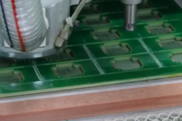
Take hole wall treatment, for example; drilling holes in ordinary PCBs is like drilling into soft soil. However, the resistance encountered by the drill bit is completely different when dealing with thick copper plates. I’ve seen some manufacturers use ordinary drill bits to process thick copper plates in order to meet deadlines. The result? The hole walls are as rough as sandpaper, and the plating layer simply won’t adhere during subsequent electroplating. This kind of compromise on details often leads to the scrapping of the entire batch of products.
The etching process is even more of a test of patience. When etching thin copper plates, the etching solution can penetrate evenly, but etching thick copper plates is like carving a solid piece of metal. Once, during a factory visit, I witnessed an interesting phenomenon: operators needed to constantly adjust the spray angle of the etching machine because the etching speed at the edge and center of the board can differ by more than two times. This reminded me of how uneven stirring in cooking results in undercooked food—the precision of the circuitry on thick copper plates depends entirely on this kind of minute manipulation.
The resin filling stage is the one most easily overlooked. I once observed an engineer examining the cross-section of a laminated board through a magnifying glass; the tiny air bubbles lurking within the crevices of the copper traces resembled dormant bombs. It was only after they adjusted the flow properties of the prepreg that the resin began to slowly seep into every nook and cranny—much like honey.
Actually, I have a little habit when choosing heavy copper PCB manufacturers: I don’t look at their equipment list, but rather go to the workshop to see how experienced workers handle defective products. Once, I saw an experienced worker using a flashlight to check the reflection angle of the hole walls at an angle; these small, experienced actions are the most reassuring. After all, even the most advanced equipment needs a human operator, and the subtle challenges in thick copper plate manufacturing often require this kind of accumulated feel to judge.
Seeing everyone getting bogged down in various parameters when discussing thick copper plate design, I think it’s better to look at the actual application scenario rather than being confined by formulas. A photovoltaic inverter project we had last year particularly illustrates this point. The client insisted on using 12 ounces of copper thickness, and during testing, we found that the local temperature was 15 degrees higher than expected.
In fact, when collaborating with heavy copper PCB manufacturers, you’ll find that they focus more on whether the overall heat dissipation solution is reasonable. During a factory visit, I witnessed an interesting comparative test: two identical 10-ounce copper samples. One had a conventional design with densely packed traces, while the other concentrated high-current paths in a specific area and provided heat dissipation channels. The latter showed a 20% lower temperature rise under full load. This made me realize that simply increasing copper thickness is less effective than optimizing heat distribution.
Current carrying capacity cannot be determined solely by table data. I’ve encountered cases where trace widths calculated to be more than sufficient according to standards still resulted in fuse failures. It turned out that multiple power modules operating simultaneously generated harmonic currents. Now, when designing, we always require clients to provide actual operating waveform diagrams, as transient peak currents can be three to four times the average.
There’s a common misconception about copper thickness selection—that thicker is always better. In reality, beyond 8 ounces, each additional ounce provides less improvement in heat dissipation and can even create challenges for the lamination process. Once, we tried a 6-ounce copper solution with thermal paste, and the results were better than simply using 10 ounces, while also reducing costs by one-third.
What impressed me most was a case study of an industrial power supply where the initial concern was that 2mm trace width wouldn’t be enough. However, after adding auxiliary heat dissipation fins to the board edge, it not only passed the 200-ampere test but also saved wiring space. This kind of flexible adjustment is more meaningful than obsessing over copper thickness, since board thickness is also a key factor affecting overall heat dissipation.
Ultimately, designing thick copper boards is like making soup—too much salt doesn’t necessarily make it taste better; the key is how the other ingredients are combined. Instead of getting hung up on a particular parameter, it’s better to communicate more with manufacturers; their accumulated failure cases are often more valuable than theoretical formulas.
I’ve always found choosing a PCB supplier quite interesting. Some clients always focus on price, looking at the apparent cost differences, but the hidden expenses from later maintenance are far less important. I remember a photovoltaic inverter project last year where they compared prices from several heavy copper PCB manufacturers and chose the lowest price. Later, due to inadequate heat dissipation, the entire project was reworked, delaying the project by two months, and the losses far outweighed the small amount of money saved.
In fact, judging whether a supplier is reliable doesn’t require looking at those fancy brochures. I usually just ask them if I can see the lamination process on-site. Good manufacturers show their differences even in the lamination process, especially when handling ultra-thick copper layers. Temperature control and pressure uniformity directly impact finished product quality. I once visited a factory where their temperature and humidity control in the workshop was incredibly meticulous; even the operators’ gloves were anti-static. These details often reflect reality more accurately than equipment specifications.
Many people think thick copper plates are simply thicker copper foil, but this understanding is too simplistic. What truly affects performance is the bonding strength between the substrate and the copper foil. For example, some manufacturers use specially treated copper blocks as localized heat dissipation units. This design has extremely high process requirements, but the effect is far better than simply stacking thicker copper, especially in high-frequency, high-power scenarios. Optimizing the heat conduction path is more important than blindly increasing thickness.
Currently, there’s a misconception in the industry of pursuing ultra-thick copper of 8oz or more. In most industrial scenarios, 4-6oz is sufficient. The key is finding the right supplier cooperation model. I prefer to cooperate with manufacturers that can provide technical support, such as those who can participate in thermal simulation discussions during the design phase and even suggest optimized wiring based on current distribution. This kind of deep collaboration is far more valuable than a simple buyer-seller relationship.
A recent case study was quite enlightening. A servo drive client, initially fixated on 20oz boards, switched to a specialized manufacturer. The manufacturer suggested embedding custom-sized copper blocks in critical areas with a 6oz substrate, resulting in a 30% cost reduction and improved heat dissipation. This made me realize that choosing a supplier isn’t about choosing specifications, but about choosing their engineering problem-solving capabilities.
Ultimately, PCB thickness is just a superficial aspect. The real barrier lies in the manufacturer’s understanding of material properties and accumulated process experience. Some smaller manufacturers can produce thick copper boards, but poor copper plating uniformity on the hole walls leads to problems after a few thermal cycles. Reliable suppliers proactively provide aging test data; this transparency is the foundation of long-term cooperation.
I’ve recently been researching an interesting phenomenon—many high-end PCB manufacturers are now focusing on heavy copper plating. This reminds me of a factory I visited last year, its workshop piled high with special boards.
I used to think PCBs were just thin layers of green paint. But seeing copper layers several times thicker than usual gives you a strange sense of solidity. The weight of these boards is reminiscent of the texture of ancient city walls.
A friend who designs power supplies complained to me about the struggles of ordinary circuit boards under high current conditions. His lab was piled high with burnt-out boards until he finally solved the heat dissipation bottleneck by trying a product from a heavy copper PCB manufacturer. Now, his team prioritizes copper thickness when designing industrial power supplies.
Artificial intelligence has already penetrated these specialized circuit board fields. I’ve seen a testing system that can adjust etching parameters in real time through thermal imaging; this dynamic optimization is far more precise than traditional processes. However, many manufacturers are still at the basic automation stage; only a few are truly using AI in the core processes of manufacturing.
Interestingly, heavy copper boards bring not only performance improvements but also a change in design thinking. Engineers are starting to plan current paths like architects consider load-bearing walls. One photovoltaic inverter project even redesigned the circuit topology to leverage the advantages of thick copper.
But these specialized boards place stringent demands on manufacturers. I once saw a multilayer board with copper thickness controlled uniformly across different areas of its cross-section, as if measured with a ruler—this requires years of accumulated process experience.
In the coming years, the explosive growth in demand for electric vehicles and energy storage will only increase the demand for circuit boards capable of handling high currents. Manufacturers mastering core technologies may see new opportunities, as the market will always need products that can build technological barriers.
I’ve always found choosing a reliable heavy-duty PCB supplier quite interesting. Many manufacturers claim to handle thick copper PCBs, but very few truly understand the process.
I remember once having a project that required ultra-thick boards exceeding 10 ounces. We contacted several so-called heavy copper PCB manufacturers, only to find they couldn’t even perform basic current-carrying capacity tests. One supplier was quite honest, telling us they could only produce 6 ounces at most, and anything beyond that depended on luck.
The key to judging a manufacturer’s reliability lies in their attention to detail. For example, when producing 10-ounce copper boards, some manufacturers proactively provide thermal cycling test reports, while others can’t even accurately calculate the board shrinkage rate. The most professional manufacturers I’ve seen have engineers who discuss wiring solutions with us, even repeatedly simulating the placement of ventilation holes. Many manufacturers like to boast about their ability to produce extremely thick boards, but thickness is just a basic requirement. What’s truly important is their ability to guarantee the uniformity of each board, especially preventing delamination during multilayer board lamination.
We once tested samples from different manufacturers, both nominally 8 ounce copper boards, and found thickness variations of ±10%. Such deviations are disastrous in high-current applications.
I think it’s better to find a partner who can consistently deliver quality within a standard thickness range than pursuing the ultimate thickness parameter. After all, most industrial applications don’t require ultra-thick boards exceeding 20 ounces; solidifying the manufacturing process in the 8-12 ounce range is far more practical.
Recently, I’ve noticed an interesting trend: some traditional heavy copper PCB manufacturers are starting to offer design support services. They not only handle production but also help customers optimize wiring solutions, which is far more valuable than simply selling boards.
Ultimately, finding a supplier is like finding a partner; it’s not enough to just look at the hardware. You also need to assess whether their technical team has the sincerity and ability to solve problems.
While collaborating with a smart wearables team to select a semiconductor flex
We often regard electronic products as a glossy whole, but ignore the
Many assume that choosing China for PCB assembly is solely about saving
- خبير في إنتاج دفعات صغيرة إلى متوسطة الحجم
- تصنيع ثنائي الفينيل متعدد الكلور عالي الدقة والتجميع الآلي
- شريك موثوق لمشاريع تصنيع المعدات الأصلية/التصنيع عند الطلب الإلكتروني
ساعات العمل: (من الإثنين إلى السبت) من الساعة 9:00 إلى الساعة 18:30