
Why is the material selection of the RF Front End PCB crucial?
The performance bottleneck of an RF front end is rarely the chip
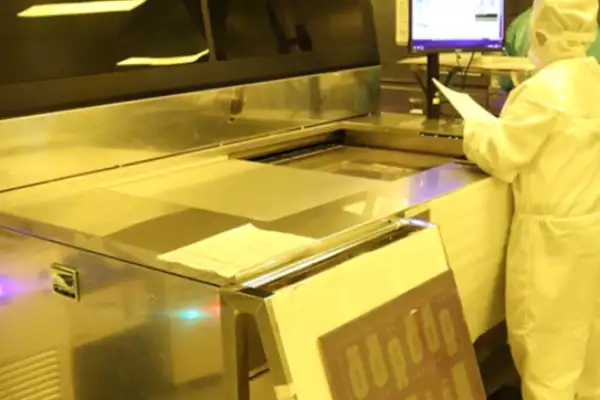
Over the years of making PCB boards, I’ve gained some insights: Many people think that drawing a good circuit diagram is all that’s needed. The real challenge lies in what happens when those lines are transformed from drawings into a physical object.
I remember once helping a client make a high-frequency board and discovering an interesting phenomenon—the same design file sent to two different factories resulted in boards with characteristic impedances that differed by 10%. Later, after observing the workshop, I discovered the problem lay in seemingly simple processes.
For example, you might design a perfectly straight line, but during actual production, the etching solution can create a subtle curve at the edge. The degree of this curve is directly related to the thickness of the copper foil used. I’ve seen people use thick copper foil for precision circuits, resulting in lines that looked like they’d been gnawed.
Now, when dealing with fine lines, I always communicate with the manufacturer beforehand about compensation. After all, each factory has different equipment parameters; some have higher etching solution temperatures, others higher spray pressures, all of which affect the final line width.
Once, we deliberately designed traces in different directions on the same board. We found that lines running along the board’s edge were always a few micrometers thinner than those perpendicular to it.
The most troublesome area was the corners of the board, where lines were always most prone to problems. Later, we realized this was because the etching solution flowed faster at the edges and more gently in the center.
I’ve now developed a habit of cutting several sample boards and carefully examining their cross-sectional shapes under a microscope after each trial production run. Although it’s time-consuming, it helps me discover many details that I hadn’t considered during the design phase.
Actually, after working in this industry for a while, you’ll find that sometimes the most inconspicuous steps are the most crucial. Like adjusting the concentration of a seemingly simple chemical solution, which might hold the key to the success or failure of the entire board’s performance.
Recently, I’ve been trying to make the compensation amount dynamically adjustable, fine-tuning the design parameters according to the characteristics of different areas of the board. Although the initial workload was larger, the yield rate has definitely improved.
Ultimately, PCB manufacturing is a process of constantly challenging oneself. What seems perfect today might reveal a new discovery tomorrow. That’s probably what makes this industry so fascinating.
Every time I see people blaming the factory for PCB problems, I want to laugh. The other day, an engineer came to me with his four-layer board complaining that the manufacturer had made the impedance 10% off. I asked him what substrate thickness he used. He stammered and said it was based on the software defaults. This is typical theoretical thinking—you haven’t even understood the material properties, yet you expect the factory to perform magic for you?
PCB manufacturing is never as simple as following drawings. I’ve seen too many people just throw Gerber files at the factory and think everything is fine. In reality, the drawing begins to distort the moment you click the export button. Photoplotter lenses have distortion, etching solution concentration fluctuates, and laminator temperatures have gradients—which of these variables can CAD software simulate? Last year, we conducted an experiment where the same batch of files sent to three factories resulted in boards with characteristic impedances differing by 15%.
Truly skilled designers thoroughly understand the manufacturing processes beforehand. For example, do you know the minimum line width achievable by mainstream PCB manufacturers in China? It’s not about looking at equipment parameters, but at their actual daily production data. Once, I chatted with a master craftsman in the workshop and discovered that their etching process tolerances were 0.5 times larger than those specified in the technical manual because the old machines had been used for eight years. You can’t grasp these details without being on-site.
Many people now overly rely on simulation software, but those beautiful color spectra are results under ideal conditions. I remember the first time I designed a six-layer board, the simulated impedance curve was perfect, like something out of a textbook. However, the measured sample was completely off at high frequencies. Later, I discovered it was due to uneven copper thickness during electroplating—a parameter not available in the simulation.
Ultimately, design and manufacturing require dialogue, not one-way instructions. You need to understand the actual operational logic of the factory—for example, why they add processes during layout and assembly, and why the plating process affects pad dimensions. These process details are often more important than theoretical calculations. Sometimes, fine-tuning the wiring spacing is more effective than replacing the substrate with a more expensive one.
Recently, an interesting phenomenon has emerged: more and more small factories are starting to offer design feedback services. This is actually a good sign, indicating that the industry is beginning to realize that problems cannot be simply blamed on the manufacturing end. After all, even the most sophisticated equipment cannot compensate for design flaws that are out of touch with reality.
Having worked in the PCB industry for so many years, what I find most interesting is not the high-end technological breakthroughs, but those seemingly insignificant small problems, such as changes in board dimensions.
Many people think this is just a matter of a few millimeters, how much impact could it have? But these tiny changes often determine the success or failure of the entire project.
I remember once we were making a 16-layer communication board. The initial design went smoothly, but problems arose during the PCB Board Manufacturing stage. Because of the complex stack-up structure and the significant differences in the expansion coefficients of different materials, noticeable dimensional changes occurred during the high-temperature, high-pressure lamination process. Although we implemented pre-compensation, the actual manufactured board was still about 0.15 millimeters larger than the design dimensions.
You might think this small error is insignificant, but for high-density designs, it’s a disaster. One BGA package had a particularly small pin pitch, and this slight deviation caused solder bridging during soldering.
We later spent considerable effort finding the root cause—it turned out that the different core materials expanded at different rates when heated during the lamination process. While the expansion and contraction of each layer was within reasonable limits, the cumulative effect exceeded our expectations.
Now, we are extremely careful about this issue when designing complex multilayer boards. In addition to standard process compensation, we make extra adjustments based on the specific stack-up structure and material properties. Sometimes, we even reserve more safety margins during the design phase.
I think the most important thing in this industry isn’t pursuing the most advanced technology, but solving these fundamental problems well. After all, even the best design is useless if basic manufacturing precision can’t be guaranteed.
Every time I encounter similar problems, I think that perhaps this is the charm of this industry—there are always new challenges waiting for us to solve. I’ve always felt there’s a misconception about PCB manufacturing—that simply handing over design files to a factory automatically produces a perfect product. The process of transforming blueprints into a physical prototype is actually quite fascinating.
I remember once designing a board that seemed perfectly normal in software simulations—but the finished product had wildly varying impedances. Later, talking to the manufacturer’s engineers, I discovered the problem lay in my choice of substrate—the dielectric constant of FR4 from different manufacturers can differ by more than ten percent.
That experience taught me a valuable lesson—the most crucial aspect of PCB board manufacturing is that the designer must understand material properties. Seemingly basic choices like the substrate type and copper foil thickness directly impact the final performance.
Now, every time I design a board, I first confirm the manufacturer’s commonly used material parameters—adjusting the simulation model to match the actual production line.
Another small detail that many people easily overlook—the solder mask opening size must have sufficient margin. I had a board where the solder mask layer coverage was too precise—a slight misalignment resulted in insufficient exposed copper on the pads—leading to rework costs three times higher than normal production.
Good PCB design should be like woodworking—it needs to allow for sanding and finishing—after all, industrial production isn’t an ideal environment.
Recently, I helped a friend modify a drone flight control board. The original design crammed all the vias directly beneath the BGA chips—saving space but greatly increasing manufacturing difficulty—ordinary factories simply can’t achieve the precision of blind and buried vias.
Later, we moved the vias to the periphery of the chips—although the board became larger—the yield rate increased from 30% to 90%—a very worthwhile trade.
Ultimately, design and manufacturing are never a relay race but a duet—you need to understand your partner’s limitations to dance the perfect dance.
Sometimes, I see novice designers getting bogged down in 0.01mm trace optimization in software—forgetting to ask the factory about their etching precision—this is putting the cart before the horse, which is a real shame.
The truly reliable approach is—after designing the board, have it prototyped by three manufacturers for comparison—record the feedback from each manufacturer—and gradually you’ll understand the characteristics of different process routes.
I’ve developed a habit—before each batch of production, I always request process control data from the manufacturer—especially the electroplating bath composition and drill bit wear records—these details often determine success or failure.
Ultimately, turning a PCB from blueprints into a physical object isn’t the real skill; achieving stable mass production is.
I’ve seen too many people oversimplify PCB design. They always think that drawing the circuit diagram is all that’s needed, until the first prototype returns and they discover numerous problems.
I remember once helping a friend check the design of a six-layer board. He confidently stated that all parameters were accurate to two decimal places, but the manufacturer reported a micrometer-level offset during lamination. This reminded me that in PCB board manufacturing, seemingly insignificant details often determine success or failure.
Many people get bogged down in theoretically perfect tolerances but ignore the dynamic factors in actual production, such as the impact of ambient temperature and humidity on the board material or the subtle vibrations of the equipment during operation—all of which are reflected in the final product.
I pay particular attention to the drilling process because it’s where unexpected problems are most likely to occur. Sometimes, errors caused by drill bit wear might be only a few tenths of a millimeter, but for high-density fiberboard (HDF), this can be disastrous, especially when the design requires a hole diameter accuracy of 0.05 millimeters. Any deviation can render the entire board unusable.
Once, we tested the processing capabilities of different manufacturers and found that the smoothness of the hole walls produced by different manufacturers for the same specifications of board material varied significantly. This directly affected the quality of subsequent electroplating.
In fact, good manufacturers make thorough predictions before production rather than rigidly adhering to the data provided by the customer. They adjust process parameters according to the material characteristics; this flexibility is key to ensuring quality.
Another easily overlooked point is the compatibility between design documents and production equipment. For example, drilling files generated by certain CAD software may have tiny rounding errors when interpreted on actual equipment. Although these errors are only a few tenths of a millimeter, they accumulate and affect the overall accuracy.
I now prefer to maintain close communication with manufacturers rather than simply sending them design documents and considering the job done. After all, they understand better what will happen on the production line.
Ultimately, PCB manufacturing is a fusion of art and science, requiring both rigorous calculations and accumulated experience. Behind those seemingly cold numbers lie countless trials and errors.
I’ve seen too many engineers treat PCB design like a drawing game. They spend weeks adjusting trace widths and optimizing component placement. These are certainly important. But the key to whether a board is usable often lies in the manufacturing process.
I remember once our team made a high-frequency circuit board. The simulation results were incredibly exciting. However, when the first batch of samples returned for testing, we found severe signal attenuation. The problem lay in the dielectric constant of the substrate. The nominal value provided by the supplier differed slightly from the actual manufactured board. This fluctuation in physical properties is something simulation software can never fully replicate.
Later, we adjusted our strategy. We proactively contacted several PCB manufacturers during the design phase, discussing substrate selection, copper foil thickness tolerances, and the actual production capacity for minimum trace widths with their engineers. These seemingly trivial manufacturing details became crucial factors in design decisions.
One case left a deep impression on me. We needed to arrange dense BGA packages within a limited space. Following conventional design rules, this was almost impossible. However, the manufacturer suggested we try a special prepreg combined with laser drilling. This combination allowed for smaller, higher-density vias. Ultimately, we achieved our design goals.
Now, for any new project, I consider manufacturing feasibility first. It’s not simply about checking if DRC rules are met. It’s about truly understanding the physical implementation behind each design choice. For example, impedance control for differential pairs depends not only on trace width and spacing but also on lamination thickness and dielectric material properties.
Good design should anticipate and mitigate potential manufacturing problems at the drawing stage. This requires designers to have a deep understanding of manufacturing processes. You can’t push all the responsibility onto the manufacturer and expect them to solve all engineering problems.
Recently, we were working on a flexible circuit board project. This time, we invited the manufacturer to participate in the design review from the beginning. They pointed out several stress concentration issues in bending areas that we hadn’t noticed. This feedback helped us avoid many potential reliability issues later on.
Ultimately, PCB design isn’t an isolated technical task; it requires close collaboration across the entire chain from concept to mass production. Every step needs to work in concert to create a reliable and economical product – this is where an engineer’s true skill is tested.
I’ve seen too many engineers create incredibly detailed and beautiful PCB designs, only to have problems arise during actual production. This reminds me of a mistake I made when I first entered the industry – I thought minimizing trace spacing was the key to success. Now I understand that the real test is understanding the manufacturing process.
The accumulation of tiny errors in PCB manufacturing can ruin an entire design. For example, you might draw a 0.2mm wide line and think it’s sufficient, but every step in the factory process will have deviations. From substrate treatment to pattern transfer to etching, each step can produce variations on the order of millimeters. These seemingly insignificant numbers, when combined, can result in a final board that’s completely different from what you intended.
One project left a deep impression on me. To save space, we pushed the via spacing to its limit. Theoretically, the calculations were feasible, but in actual production, a tiny misalignment during drilling directly caused short circuits between adjacent via walls. Later I learned that while drilling machines are highly precise, the expansion and contraction of the sheet metal during processing due to temperature and humidity fluctuations cannot be completely avoided.
Now, when communicating with my team, I focus more on the process window than the theoretical limit. After all, what experienced workers on the production line often say—”can be done”—and “can be done consistently”—are two different things. For example, the design software might show perfect alignment of the inner layer circuitry, but differences in the thermal expansion coefficients of the materials during lamination can cause micron-level misalignment. This misalignment, amplified by subsequent electroplating, etching, and other processes, can lead to impedance mismatch issues in the finished product.
Good design should allow for breathing room in manufacturing. I like to leave an extra 10% to 15% margin in critical areas. This isn’t about being conservative, but about respecting the laws of production. After all, what we ultimately want are reliable products that can be mass-produced, not perfect samples in a lab.
Recently, I helped a client redesign the layout of a Bluetooth module. The original design had the antenna traces drawn very finely along the board edge. However, during mass production, uneven etching caused significant performance fluctuations in each batch of antennas. Increasing the trace width by 20% and adjusting the copper foil distribution immediately stabilized the situation. This adjustment might seem like a regression on the circuit diagram, but it’s actually a step towards manufacturability.
Finally, PCB design isn’t about battling software, but dealing with physical laws. Truly knowledgeable engineers see manufacturing errors as part of the design parameters; those millimeter-level variations aren’t obstacles, but rather realities that need to be understood and managed.
I’ve always felt that the most interesting aspect of PCB manufacturing is the intricacies hidden behind seemingly simple processes. Take electroplating, for example. Many people think that simply soaking the board in a solution will ensure uniform copper plating, but in reality, uneven current distribution makes the entire process highly unpredictable.
I recall once testing the effects of vias with different aspect ratios and discovering that when the via diameter became too small, the flux flow decreased, and the copper layer in the center of the via was significantly thinner than at the opening. This is particularly dangerous in designs requiring high current carrying capacity, as increased local resistance can lead to overheating.
Regarding copper thickness control, I’ve noticed many engineers overlook the pretreatment of the substrate surface. In fact, the roughness of the substrate directly affects plating adhesion; excessive smoothness can actually cause delamination. We once tried adding a micro-etching step before chemical copper plating, which resulted in a nearly 30% increase in yield.
More and more factories are now emphasizing pulse plating technology. This method of alternating current direction can indeed improve metal deposition in deep vias. However, it’s crucial to note that pulse parameters need to be adjusted in real-time according to the board thickness; fixing parameters may create new unevenness.
Recently, I encountered a very interesting case: after three years of use, open circuits began appearing in the vias of an industrial control board. Disassembly and analysis revealed an imbalance in the additive ratio during electroplating, leading to a hidden problem in the copper layer’s grain structure. These microscopic issues often only become apparent after long-term aging and are more difficult to detect than obvious insufficient thickness. In fact, the most demanding aspect of PCB board manufacturing is this meticulous attention to detail. Even the slightest deviation in each step can be amplified in subsequent processes, ultimately affecting the reliability of the entire batch. Sometimes I feel this industry is more like conducting a chemistry experiment, requiring constant adjustment of various parameters to find the optimal balance.
Speaking of balance, I think the most difficult aspect is balancing cost control and quality assurance. For example, increasing plating time can improve the coverage of holes with large aspect ratios, but it reduces production efficiency. In such cases, standards need to be tailored to the actual application scenario of the product, rather than blindly pursuing the highest specifications.
These experiences have taught me that good manufacturing processes are not about blindly copying standard procedures, but about flexibly adjusting to specific needs. After all, the design goals of each circuit board are different; only by understanding the underlying physical principles can truly reliable products be made.
The performance bottleneck of an RF front end is rarely the chip
A poorly designed Servo Controller PCB can lead to motor jitter, overheating,
When data centers upgrade their GPUs, the real bottleneck often hides in
- خبير في إنتاج دفعات صغيرة إلى متوسطة الحجم
- تصنيع ثنائي الفينيل متعدد الكلور عالي الدقة والتجميع الآلي
- شريك موثوق لمشاريع تصنيع المعدات الأصلية/التصنيع عند الطلب الإلكتروني
ساعات العمل: (من الإثنين إلى السبت) من الساعة 9:00 إلى الساعة 18:30