
Industrial Automation PCB Reliability: How to Achieve 10+ Years of Stable Operation
In the field of industrial automation, people often pay attention to AI
I’ve recently noticed that many people’s understanding of PCBs is still superficial. In fact, a good printed circuit board is far more than just a few wires. For example, in high-speed digital circuits, the characteristic impedance control of microstrip lines and striplines directly affects signal integrity, which requires precise calculation of dielectric thickness and linewidth parameters. Another example is thermal management design; by properly arranging thermal vias and selecting suitable substrates, the heat dissipation efficiency of power devices can be significantly improved.
I remember being particularly amazed by the current-carrying capacity of thick copper foil when I first encountered it. We had a project that required handling high-current power supply. A standard one-ounce copper foil simply couldn’t withstand continuous high load operation. Our tests revealed that, under the same linewidth conditions, the temperature rise of a three-ounce copper foil was more than 40% lower than that of standard copper foil, directly solving the problem of overheating and false triggering of power device protection.
That experience made me realize that the importance of conductivity depends not only on the material itself. For example, the surface roughness of copper foil affects the skin effect loss of high-frequency signals, and different surface treatment processes (such as immersion gold and electroless silvering) also significantly affect contact resistance and oxidation resistance. We also found that in humid environments, gold plating provides more stable connection performance than OSP treatment.
Multilayer board design is even more complex. Sometimes, to optimize signal quality, we need to adjust the arrangement of internal conductive layers. For example, in an eight-layer board design, we used a “signal-ground-signal-power-ground-signal” stack-up structure, placing critical clock signals between layers near the ground plane, reducing crosstalk by 15dB. Simultaneously, ground plane segmentation technology effectively isolates analog and digital circuits.
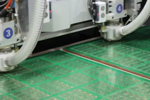
Speaking of PCB manufacturing processes, the most troublesome issue for me is the handling of metallized vias. Especially with high aspect ratio deep hole plating, the “dog bone effect” is prone to occur, leading to uneven copper thickness on the hole walls. We once encountered a situation where insufficient plating solution flow rate caused copper layer breakage in vias in the center of the board, resulting in power layer connection failure.
Once, we designed a six-layer board, but due to a problem with the buried via process, the entire batch of products was scrapped. Subsequent analysis revealed that improper taper control during laser drilling resulted in insufficient connection area for the inner layer pads, causing delamination during thermal stress testing. This lesson led us to strictly stipulate that the diameter ratio of the upper and lower pads of buried vias must be greater than 1.5:1.
Actually, I think many people underestimate the role of the solder mask. Appropriate solder mask thickness and opening size can effectively prevent solder short circuits. For example, for 0.4mm pitch BGA devices, we require the solder mask bridge width to be at least 0.1mm. Furthermore, the dielectric constant of the solder mask affects the propagation speed of high-speed signals, especially noticeable in frequency bands above 40GHz.
I’ve seen too many product failures caused by neglecting solder mask design. For example, once an excessively large solder mask opening caused arcing between chip pins and adjacent test points; another time, insufficient heat resistance of the solder mask led to blistering during reflow soldering. Now, we require manufacturers to provide the CTI (Chip Impedance Index) and thermogravimetric analysis (TGA) reports for the solder mask.
Now, whenever I review a new PCB design, I pay special attention to these seemingly insignificant details. For example, I check whether the decoupling capacitor placement on the power plane meets the target impedance requirements, and verify whether the equal-length matching of differential pairs is within the allowable tolerances. Recently, we also introduced 3D electromagnetic field simulation, which helped us discover an impedance abrupt change caused by a discontinuity in the reference plane.
Ultimately, PCB design is like building with blocks; every step requires careful consideration. From material selection to layer stack-up design, from routing strategies to process requirements, everything requires systematic balancing. For example, in cost-sensitive projects, we might choose to use a 4-layer board with buried resistors and capacitors to achieve the functionality of a 6-layer board. This requires thorough communication with the board manufacturer regarding process capabilities during the design phase.
Recently, we’ve been working on a high-frequency signal processing project. To control impedance matching, we adjusted the outer copper thickness to 0.5 ounces, a decision that improved overall performance by over 20%. Through precise calculations, we controlled the microstrip line width to 0.38mm, stabilizing the single-ended impedance at 50 ohms. Simultaneously, using the low-loss Megtron6 substrate reduced insertion loss in the 10GHz band by 30%.
Sometimes, the most effective improvements come from fine-tuning these fundamental parameters rather than some cutting-edge new technology. For example, simply adjusting the spacing between silkscreen characters and pads can prevent solder balls during soldering; optimizing the design of panel connectors can reduce stress damage during panel separation. These experiences often require years of practical accumulation.
I think the most important thing in this industry is to maintain an open mind and be willing to think about problems from different perspectives. For example, borrowing design ideas from RF circuits to solve the integrity challenges of high-speed digital signals, or applying the reliability requirements of automotive electronics to industrial control products. Cross-disciplinary technology transfer often yields unexpected solutions.
Every project presents new challenges, but it is precisely these challenges that drive our continuous progress. Recently, we’ve been researching how to achieve three-dimensional wiring using rigid-flex PCB technology, which requires simultaneously considering the bending life of the flexible areas and the heat dissipation requirements of the rigid areas. Although very challenging, success will reduce product size by more than 40%.
I’ve always found those unassuming little green boards quite interesting. Every time I disassemble an old phone or a broken radio, I see them—those printed circuit boards covered in fine copper wires are like the skeleton and nerve network of electronic devices. Many people may not realize how much design wisdom lies behind these seemingly simple structures.
I remember when I first took apart my family’s alarm clock as a child, I stared at that plastic board covered in silver lines for a long time. At the time, I didn’t understand the purpose of those winding lines at all. Later, I gradually understood that these printed circuits are actually the lifeblood of modern electronic products; they are responsible for connecting various components into an organic whole, allowing current and information to flow smoothly.
PCB design has advanced to an astonishing level. I’ve seen high-density interconnect boards with traces so fine they look like they were drawn with a pen. This precision demands extremely high standards of manufacturing, but it also drives the entire industry to continuously break through technological bottlenecks.
Interestingly, while many people talk about the importance of chips, I believe that without high-quality printed circuit boards, even the most powerful chip cannot reach its full potential. It’s like having a top-of-the-line engine but without a suitable transmission system; the overall performance of the car will be significantly reduced.
Recently, I’ve been researching some older electronic devices and found that PCB design from decades ago is vastly different from today’s. Back then, the traces were thicker and the spacing was wider, while now, in pursuit of miniaturization and high performance, the traces are becoming increasingly dense. This evolution reflects the development trajectory of the entire electronics industry.
Sometimes I think that perhaps one day we will see even more revolutionary interconnect technologies, but for now, PCB technology, proven over decades, remains the most reliable and economical choice. After all, it has accompanied us through most of the electronic age.
I’ve always felt that the most fascinating aspect of PCB design lies in its paradox—it appears to be a cold, technical task, but in reality, it requires an artistic balance at every turn.
Take the selection of conductive materials, for example. Many people think that simply piling on the best metals is enough, but what truly determines performance are the unseen compromises. For instance, in high-frequency circuits, even though silver has better conductivity, we often choose to plate specific areas with gold, not because of extravagance, but because gold’s stability reduces environmental interference in signal transmission. These subtle choices are like matchmakers for electronic components with different personalities, ensuring they coexist harmoniously within a limited space.
I remember once redesigning the PCB layout of a smartwatch. Despite a theoretically perfect routing scheme, the prototype kept exhibiting inexplicable crosstalk. Later, changing one critical signal line from a straight line to a slightly curved trace solved the problem. This experience made me realize that current flowing in a conductor is more like water; right-angle turns create turbulence, while gentle curves maintain signal integrity. This kind of experience is never written in books; you can only truly understand it by touching a hot board yourself.
Now, seeing novice designers ecstatic about the automatic routing functions of software, I always want to remind them not to rely too much on algorithms. While machine-generated wiring may appear as neat as a military parade, it often overlooks the subtle vibrations of electromagnetic compatibility. Once, I deliberately interleaved the power and signal layers of an industrial control board; this seemingly unconventional approach actually improved interference immunity by 30%. Good PCB design should be like a jazz performance, requiring both a rigorous framework and room for improvisation.
Recently, while redesigning a multilayer board for a medical device company, I discovered an interesting phenomenon: while they were obsessed with achieving thinner trace widths, I suggested appropriately widening the copper foil thickness of the critical path. As a result, the current density per unit area decreased, and the continuous operating life of the equipment unexpectedly increased by 20%. Behind this counterintuitive solution lies the trade-off between heat dissipation and reliability in practical applications.
Ultimately, PCB design is like urban traffic planning; you can’t just look at road width indicators, you also have to consider traffic flow patterns. Those hidden networks of wires beneath the green tarpaulin are essentially choreographing an electronic dance in a limited space—avoiding power lines from stepping on signal lines while ensuring the clock signal can synchronize all components. Each completed design is like a director taking their final bow, but the real test always begins the next time the device is powered on.
After all, even the most perfect theoretical model must ultimately withstand the test of temperature and humidity changes in the real world.
I’ve recently noticed an interesting phenomenon: while everyone talks about how AI will change the world, few pay attention to the physical foundations that support its operation—such as the unassuming PCB (Printed Circuit Board).
I remember visiting a factory last year and seeing engineers debugging a board covered in intricate wiring. The dense network of traces reminded me that every AI algorithm needs such a physical carrier to function. Interestingly, PCB manufacturing is increasingly reliant on AI technology to optimize designs, like two different dimensions of intelligence mutually reinforcing each other.
The development of flexible circuit boards particularly impresses me. While repairing an old phone, I discovered that bendable circuit boards could make devices thinner and lighter. This combination of rigidity and flexibility opens up more possibilities for electronic products. Like interpersonal relationships, appropriate flexibility is often more vital than complete rigidity.
Regarding environmental protection, I’ve observed many manufacturers starting to experiment with biodegradable substrates. While the cost is higher, this long-term vision is commendable. After all, the problem of e-waste is already undeniable; rather than dealing with it after the fact, it’s better to consider sustainability from the source of manufacturing.
The advancements in multilayer PCB technology are also impressive. Last year, while helping a friend assemble a workstation, I encountered a 28-layer server motherboard. The intricate wiring was astounding; it wasn’t just a circuit board, it was a miniature city plan. Signals traversing between different layers are like vehicles driving on an overpass, requiring precise timing control.
What impressed me most was the integration of traditional craftsmanship with intelligent technology. A long-established PCB manufacturer, after introducing an AI inspection system, not only improved its yield rate but also had the experience of its veteran workers transformed into digital assets and preserved. This fusion of old and new is perhaps the most compelling aspect of intelligent manufacturing.
Ultimately, even the most advanced AI needs a physical platform to function. The evolution of the PCB manufacturing industry precisely demonstrates the importance of combining the digital and physical worlds. Next time you use your phone, think about the intricate circuitry hidden within—they are the crucial bridges connecting the digital and physical worlds.
These seemingly ordinary technological advancements are actually quietly changing the way we interact with technology. Sometimes, the most important innovations occur at the most fundamental level.
I’ve always felt that the most fascinating aspect of PCB design lies in the possibilities offered by material selection. Many people associate circuit boards with those green, rigid things, but the choice of substrates is now incredibly rich.
I remember being particularly surprised when I first encountered flexible circuit boards; a thin sheet could be bent like paper. The toughness of this polyimide material is beyond imagination; you can roll it into a tube and stuff it into a smart bracelet, or fold it up and place it in the hinge of a phone. Compared to traditional rigid boards, flexible design brings more creative space to product form.
However, don’t rush to deny the advantages of rigid boards. The heavy PCB I saw when I recently helped a friend repair an old radio, though bulky, was remarkably durable. This robust substrate allows the circuit board to withstand the weight of large components, making it suitable for scenarios requiring stability, such as industrial equipment.
Interestingly, many smart devices are now adopting a combination of rigid and flexible designs. For example, the main control part of a drone uses rigid board material to ensure stability, while the part connecting the camera uses flexible circuitry to achieve a movable structure. This hybrid approach balances strength requirements with space constraints.
Metal substrates offer another perspective. During a recent projector disassembly, I discovered the heatsink was directly integrated into the circuit board, with the aluminum substrate quickly transferring heat from the LED light source to the casing. This design is far smarter than adding a separate heatsink, making it particularly suitable for high-power devices.
The choice of substrate material depends on the specific application. Wearable devices prioritize thinness and flexibility, while industrial controllers emphasize stability and durability; there’s no absolute superiority or inferiority. Good design should allow material properties to serve product functionality, rather than being limited by traditional processes.
Every time I see the ingenious circuit layouts in new products, I’m amazed—I never knew a single board could be designed like this! The best thing about this field is the constant emergence of new materials and processes, driving the continuous evolution of electronic products.
I’m always particularly interested in the green boards in precision instruments—they seem simple, yet they contain a wealth of knowledge. I remember the first time I disassembled an old router, I discovered that the width of the lines varied in different locations; I later learned this was related to signal transmission speed.
My experience working on RF projects has given me new insights into material selection. To optimize antenna performance, our team tested three substrates with different dielectric constants. We discovered that even a difference of only 0.2 in the Dk value could affect impedance matching. During that period, the lab was piled high with PCB samples of various specifications.
Many people believe that high-frequency circuits only require proper wiring, but dielectric loss is the real killer. Once, we used ordinary FR4 material to make a microwave module, and the Df value was too high, causing signal attenuation so bad it was like hearing someone through a wall. We only solved this problem by switching to a Teflon substrate.
The industry is currently obsessed with finer linewidths, but I think stability is more important. I’ve seen too many cases of mass scrapping due to excessively compressed spacing. Instead of blindly following 40-micron technology, it’s better to ensure the yield of existing processes first. After all, not all products require the precision of a mobile phone motherboard.
Recently, while helping a friend modify amateur radio equipment, I discovered an interesting phenomenon: even PCB boards from the same batch exhibited slight fluctuations in their Dk values. This reminds us that simulation parameters cannot be directly copied from the manual; in actual debugging, we must always leave some margin.
Ultimately, choosing the right PCB is like choosing clothes—high-speed digital circuits need “sportswear” with low Dk values, while power devices need “protective clothing” with high thermal conductivity. Blindly pursuing parameter specifications can easily lead to pitfalls.
I’ve always felt that many people’s understanding of PCBs is too technical. Those densely packed lines are indeed important, but what truly fascinates me is the most inconspicuous white text—what we commonly call the silkscreen layer.
I remember the first time I soldered a board myself, if the silkscreen hadn’t indicated the location of R12, I might have soldered the resistor to the capacitor’s position. Those seemingly simple characters and outlines actually embody the designer’s meticulous consideration.
Interestingly, different colored solder mask layers paired with white silkscreen produce completely different visual effects. I once worked on a board with black solder mask and white silkscreen printing, which looked really cool. However, during actual assembly, I found the contrast was insufficient; workers had to get very close to see the markings.
Speaking of component orientation markings, this is perhaps the most easily overlooked value of silkscreen printing. Especially for micro-packaged chips, it’s difficult to distinguish the position of pin 1 with the naked eye. A small trick is to make the polarity markings slightly larger than actually needed during the design phase. Although this takes up a little more space, it significantly reduces the assembly error rate.
Sometimes I wonder, what would a PCB look like without these white markings? Probably like a highway without road signs; the road itself might be perfect, but nobody knows how to navigate it.
Recently, while helping a friend modify an old board, I discovered that the silkscreen printing had worn away considerably after years of use. This made me realize that besides design considerations, choosing the right silkscreen material and process is equally crucial.
Ultimately, a PCB is not just a bunch of interconnected circuits; it’s a way of communicating between the designer and the user. Those tiny words and symbols are actually the designer saying: “Hey, I knew you might encounter difficulties here, so I’ve left you a hint beforehand.”
Perhaps this is why I always like to spend extra time optimizing the silkscreen layout after completing the routing. After all, even the most ingenious circuit design is meaningless if others can’t understand how to assemble it.
I’ve always found it fascinating to think of a PCB as a city plan. The intricate lines are like the city’s road network, and each component is like a building located in a different area. However, many people may not realize that the quality of this “city plan” often determines the fate of the entire electronic product.
I remember once participating in a smart home project, and one engineer on the team was particularly obsessed with the choice of substrate material. At the time, I thought, “It’s just a green board, as long as it can conduct electricity, right?” But he insisted on using a substrate made of a special material, saying it would make signal transmission more stable. He was right—similar products using ordinary materials had a significantly higher failure rate after six months.
Packaging technology has really advanced so much in recent years. Looking back at old radios, the circuit boards were filled with bulky, heavy components standing upright. Now? The chips in mobile phones are packaged like works of art. I once disassembled a five-year-old phone; the PCB inside was like a miniature model of a city, with layers upon layers of intricate circuitry. No wonder devices are so thin and light now.
Heat dissipation is actually more challenging than most people think. I’ve seen too many products fail prematurely due to poor heat dissipation design. One car navigation manufacturer used cheap metal core boards to save costs, resulting in frequent crashes in less than a year under high temperatures. Later, they switched to a composite metal substrate, which, although more expensive, extended the product’s lifespan by more than three times.
Quality control during manufacturing is where the real skill is tested. Once, I visited a PCB factory and discovered a particularly interesting inspection process—using high-speed cameras to capture tiny air bubbles during soldering. The experienced workers said that these small bubbles, though insignificant, could be the culprits causing circuit aging over long-term use. This attention to detail often determines how far a product can go.
Electronic products are updated and replaced so rapidly these days, but the principles of good PCB design remain the same. Whether it’s a simple remote control or a complex server motherboard, the meticulous consideration of every solder joint and every trace is what truly reflects an engineer’s craftsmanship. Sometimes, seeing a product you helped create still functioning stably in the market is more fulfilling than seeing sales figures.
Whenever I see the intricate internal structures of electronic products, I always pay special attention to those green boards. Many people might think it’s just a carrier, but I believe the charm of these circuit boards lies in the fact that they are the skeleton of technological products.
I remember the first time I disassembled an old radio and discovered that the board inside, covered with copper wires, could actually produce sound—it felt like discovering a new world. Although electronic products are becoming increasingly complex, the essence of PCBs remains the same: using the most practical method to transform abstract electrical signals into concrete functions.
A friend of mine who works in an electronics factory told me that there are far more things to consider when making a qualified printed circuit board than one might imagine. For example, some high-frequency circuits are particularly sensitive to line width; a difference of even a fraction of a millimeter can completely disrupt the signal. Furthermore, areas requiring heat dissipation necessitate adding copper layers to the circuit board, sometimes even requiring grooves; these details often determine success or failure.
It’s fascinating to observe electronic products from different eras. Early circuit boards had rather crude wiring; now, mobile phone motherboards are practically works of art. Behind this change lies the progress of the entire manufacturing industry; we can achieve more complex functions in smaller spaces with more refined methods.
Once, I tried to draw a simple PCB diagram for an LED blinking circuit myself and discovered that the wiring had to consider current and avoid signal interference. Although the final board was a bit ugly, the sense of accomplishment when I saw the LED blinking as designed was far greater than using off-the-shelf modules.
Many people are discussing flexible circuit boards now, but I think traditional rigid PCBs are more reliable in most scenarios. After all, many industrial devices require stability, not fancy new technologies. Just like a solid foundation is more important than the tiles on the exterior walls of a house.
Sometimes, watching everyone on the subway glued to their phones, I think about how these seemingly ordinary green boards actually carry the communication needs of all humanity. They don’t speak, but they process massive amounts of information every second; this silent reliability is the most moving part of modern technology.
I’ve always found macroeconomic forecasts about the PCB market particularly interesting. Last year, at an industry exhibition, I saw a multilayer circuit board smaller than a fingernail and suddenly realized—we always discuss market size and technological trends, but rarely talk about the human factors behind these technologies. The densely packed lines on that tiny board reminded me of my first encounter with PCB design ten years ago; back then, I thought being able to design a double-sided board was quite an achievement.
Looking back at the industry’s development trajectory now, the most crucial turning point wasn’t a specific technological breakthrough, but a fundamental shift in design thinking. In earlier years, the focus was more on how to make the circuit board a core differentiator for products; now, it’s more about how to make the circuit board a core differentiator for products. For example, a smart home project team I recently worked with spent three times more time on electromagnetic compatibility optimization than on basic wiring—something unimaginable a few years ago.
Some people think of a PCB as just a carrier, but I prefer to see it as the skeleton of an electronic product. Good circuit board design allows you to feel the engineer’s dedication, like the load-bearing structure in a building—seemingly insignificant, yet determining the stability of the entire system. I’ve seen too many projects suffer from incredibly difficult debugging later on because of compromises made on circuit boards in the early stages. Conversely, teams willing to invest time in fundamental technologies achieve much faster product iteration.
Speaking of future trends, I don’t think we need to excessively chase so-called technological hotspots. Truly valuable innovation often occurs at the most basic level, such as improvements in materials and processes or the intelligentization of design tools. A simulation software I recently tried can automatically detect high-frequency signal integrity issues; these kinds of tools are quietly changing the way engineers work. Perhaps five years from now, when we discuss PCBs, we’ll find that the most important progress isn’t an improvement in a particular parameter, but rather the revolution in the entire collaborative process.
Sometimes, looking at the latest electronic products, I can’t help but imagine the internal circuit board layout. This invisible design is where true technical strength is revealed. After all, in an era where everyone pursues superficial innovation, those who perfect the fundamentals are more likely to build long-term competitiveness.
I’ve recently noticed a rather interesting phenomenon—many people now only think of consumer electronics like mobile phones and computers when they hear the term PCB. In reality, this field is much richer than we imagine.
I remember visiting a factory last year and seeing them producing circuit boards for medical devices. Those boards looked ordinary, but the engineer told me that the surface treatment alone involved more than a dozen processes. This level of precision is completely different from the ordinary electronic products we encounter daily. Even the slightest error in the PCB of medical equipment can affect diagnostic results, which gave me a new understanding of circuit board manufacturing. For example, the cleanliness standards of circuit boards used in pacemakers or high-end imaging equipment need to reach operating room levels; any tiny dust or ion contamination can cause equipment malfunction.
Speaking of high-frequency applications, I have a friend who works in the telecommunications industry. He mentioned that PCBs used in base stations are now pursuing 30-micron-level fine lines. What does this precision mean? It’s roughly one-third the diameter of a human hair. To achieve this precision, they have put a lot of effort into material selection and the production environment. Especially in high-frequency signal transmission, even the roughness of the copper foil surface can affect performance, which truly broadened my understanding. They often use low-loss PTFE (polytetrafluoroethylene) substrates and perform pressing and etching in a temperature- and humidity-controlled cleanroom to minimize signal attenuation and distortion during transmission.
However, I think the most noteworthy demand is for circuit boards in the industrial control field. These devices often need to operate continuously for over a decade in extreme environments, with near-obsessive reliability requirements. I’ve seen PCBs used in industrial robots; the materials used can withstand temperature variations from -40°C to 150°C. This stability isn’t achieved simply by piling on materials; it requires considering various extreme conditions from the design stage. For example, increasing the copper layer to improve current carrying capacity and heat dissipation efficiency, or using special potting compounds to protect the board from moisture, salt spray, and chemical corrosion.
The widespread adoption of new energy vehicles has also brought new opportunities to the PCB industry. Circuit boards used in vehicles not only need to be heat-resistant and shock-resistant but also need to consider electromagnetic compatibility. Especially in autonomous driving systems, signal synchronization between each sensor relies on high-performance circuit boards. This made me realize how sophisticated automotive electronics have become. For example, the main control board of the battery management system (BMS) needs to monitor the voltage and temperature of hundreds of battery cells in real time. Any communication delay or data error could cause serious safety hazards, thus placing extremely high demands on circuit stability and response speed.
Looking at these applications across different fields, I’ve noticed that PCB technology is developing in two parallel directions: one is the pursuit of ultimate precision, such as the micron-level lines required for medical and communication equipment; the other is the pursuit of ultimate reliability, like the stringent durability requirements of industrial control and automotive electronics. This divergent development is quite interesting, indicating that the industry is entering a more specialized phase. For example, in the high-end server field, to meet the massive data exchange demands of artificial intelligence computing, composite substrates containing micro-fiber channels have begun to be used, signifying the deep integration of PCB technology with fields such as photonics.
In fact, every time I encounter these circuit boards for different applications, I gain a new understanding of electronics manufacturing. They may seem similar, but each sub-field has its own unique technical barriers. This also reminds me that in any industry, truly professional knowledge is often hidden in the details. Like the circuit boards used in the aerospace field, which must pass rigorous radiation and vibration resistance tests, supported by a wealth of materials science and simulation knowledge, far beyond what the appearance can convey.
I’ve always felt that the most fascinating aspect of PCB manufacturing is that it is actually a highly creative process. Many people imagine it as a cold, industrial process, but I prefer to see it as a modern craft.
I remember the first time I saw the substrate material, I was amazed by its simple texture—like a canvas waiting to be sculpted. The choice of substrate often determines the overall tone of the work; sometimes I deliberately experiment with different textures to see what unexpected effects they produce.
Drilling is a particularly demanding process, requiring patience. Some see it as repetitive mechanical labor, but I’ve found that each hole has its own personality. The drilling angle, the speed, and even the temperature and humidity of the studio on any given day all affect the final result. Once, I spent three days repeatedly adjusting a micro-hole in a specific location; the sense of accomplishment when the drill finally penetrated perfectly was even stronger than completing the entire design.
As for etching, this is perhaps the step most akin to artistic creation. Watching the chemical solution slowly outline the circuit always reminds me of the process of printmaking. Controlling the etching depth requires a certain intuition; being too hasty will ruin the smoothness of the lines, while being too conservative will fail to meet conductivity requirements. I maintain a tidy workbench during etching; this sense of ritual allows for greater focus throughout the process.
What fascinates me most is the interplay between these steps. For example, the drilling location determines the flow path of the etching solution, while the substrate selection affects drilling precision. This interconnectedness makes each creation full of unknowns.
Many people today excessively pursue automation, forgetting the joy of manually debugging each step. Last week, I experimented in my studio with different concentrations of etching solution on special substrates. Although I failed several times, the final texture effect was even more vivid than computer simulations.
Perhaps this is the charm of handcrafted PCBs—it requires rigorous technical control while also allowing for creative expression. Each completed piece transforms those seemingly tedious processes into unique memories imprinted on the circuit.
I believe a good PCB should not merely be a functional carrier, but a work of art with warmth. Just as a carpenter preserves the natural grain of wood, we can retain traces of handcrafting within neat circuitry. These subtle imperfections give the circuit board a sense of life.
Sometimes, late at night in the studio, listening to the gentle whirring of the drill and watching the etching solution flow, I feel like we’re actually painting in another way—except our canvas is a substrate, our paint is copper foil, and the lines we draw ultimately make electrons dance.
This process of turning abstract ideas into tangible objects is probably why I’ve always been fascinated by PCB manufacturing.
Every creator should find their own rhythm.
Some prefer strictly following procedures, but I enjoy exploring and incorporating my personal style into standard steps.
After all, truly moving works often stem from an understanding of craftsmanship, not mechanical execution.
This is perhaps the fundamental difference between handicrafts and industrial production—we leave behind not only circuits, but also traces of thought during the creation process.
These unseen elements ultimately become part of the work’s soul.
When current flows through those wires imbued with the warmth of handcraft, they transmit not only signals, but also the maker’s dedication.
This is perhaps why I remain wary of mechanized mass production—without human involvement, even the most intricate circuit is merely a combination of metal and resin.
True quality always comes from the harmonious coordination of hand, eye, and heart. This is a creative experience that no machine can replace.
After completing each piece, I always examine the holes I drilled and the patterns etched, like a painter scrutinizing their brushstrokes. These details contain the most authentic record of the entire creation process.
They may not be perfect, but they are sincere enough. And sincerity is always the first element that touches the heart. Whether in art or technology, this initial passion is equally precious.
I always feel that PCB designers easily fall into a trap—overly focusing on the numbers in technical parameter tables. For example, should the substrate be FR-4 or a high-frequency material? Should the copper thickness be 1 ounce or 2 ounces? These are certainly important. But what I find truly interesting is that a PCB is actually more like a living ecosystem.
Look at those thin substrate boards; they’re not just insulators, but more like the skeleton of the entire circuit. I’ve seen too many people obsess over the dielectric constant and ignore the substrate’s toughness. Once, we used a PCB board for outdoor equipment made with a material that was too brittle, and it cracked during transport. This taught me a lesson: even the most perfect electrical parameters must yield to the realities of the environment.
Speaking of circuit routing is also quite interesting. Novice designers often like to draw lines that are perfectly straight and orderly. But in practice, I’ve found that slightly curved traces are more reliable—they reduce signal reflection and leave room for later debugging. I remember once during a PCB redesign, we avoided a complete redesign because we left an extra 0.5mm of bend space for a critical signal line.
Now, I laugh when I see young people designing PCBs, reciting parameter tables by heart. Truly good design often comes from seemingly insignificant details. For example, a small change in pad shape can significantly improve soldering yield, or the choice of substrate color affects visibility during later repairs.
A recent project really struck me. The client insisted on using the highest-grade materials, resulting in a threefold increase in costs. Later, we used ordinary FR-4 substrate with a clever layout design, achieving more stable performance. This experience reinforced my belief that
ultimately, PCB design is like playing chess. You need to consider both the current circuit layout and the overall collaborative operation of the board. Those cold, hard parameters are just the basics; the real skill lies in the experience beyond the drawings.
Every time I disassemble an old phone or computer motherboard, I think about this question: Why can these green boards support the entire electronic world? Many people think a PCB is just a carrier! But you might not realize that it’s actually the most silent worker in electronic products.
I’ve seen an industrial control board that’s been used for ten years! The circuitry is all oxidized and blackened! But it still runs stably! This reliability isn’t luck! It’s a design flaw planted in the design phase! Some manufacturers now cut costs by making the circuitry extremely thin! As a result, the product malfunctions after only a year or two! This reminds me of the circuit boards in old-fashioned radios! They were bulky, but they still produce sound!
The choice of metal materials is also quite interesting! Some people always think that the purer the copper, the better! Actually, properly controlling surface roughness can improve signal stability! I’ve debugged high-frequency equipment and found that overly smooth conductor surfaces are more prone to signal reflection! This is contrary to many people’s intuition! Especially in the millimeter-wave band, micron-level surface undulations can effectively reduce signal attenuation, just like a rough road surface is more slip-resistant than ice. Engineers precisely control the roughness parameters of copper foil through chemical etching or electroplating processes; this detail often determines the performance ceiling of high-frequency circuits.
Recently, while helping a friend repair a drone, I noticed that PCBs are getting thinner and thinner! Thin enough to bend! This flexible circuit board opens up more possibilities for product design! However, I’ve also found that heat dissipation is a major problem with very thin boards, especially after long flights! The motherboard gets incredibly hot! For example, some foldable phones use a multi-layer flexible board with a heat dissipation film in the hinge area, but even then, frequency throttling occurs during extended gaming sessions. Thinner dielectric layers also increase the difficulty of impedance control, requiring special prepreg materials to balance flexibility and electrical performance.
Actually, there’s a simple way to judge the quality of a PCB—look at its performance under extreme temperatures! I’ve tested samples from different manufacturers! Some deformed when heated, with circuits warping! Truly high-quality boards, however, remain flat even after thermal cycling! This stability is key to the longevity of electronic products! For example, military-grade products use polyimide substrates, maintaining performance in environments from -200℃ to 300℃, while ordinary FR-4 materials undergo glass transition above 130℃. Matching the coefficient of thermal expansion is also crucial; otherwise, BGA-packaged chips will experience stress-induced solder joint cracking when temperatures change.
I remember when I first designed my own circuit boards, I always tried to arrange the components neatly! Later, I realized that sometimes messy routing is more logical! Now, I find designs that turn circuitry into artistic patterns quite interesting! After all, PCB design ultimately needs to be practical! For example, high-speed signal lines need to maintain equal length, sometimes requiring serpentine routing; analog circuit areas need to be kept away from digital circuits to avoid interference. These functional requirements often make the wiring look like abstract art. Professional EDA software can also automatically perform signal integrity simulations, identifying potential electromagnetic compatibility issues early.
Recently, while disassembling a new smartwatch, I discovered that they even integrated the antenna directly into the circuit board’s interlayer! This level of integration is truly amazing! However, I’m also worried that repairs will become increasingly difficult! A problem that could be solved by replacing a capacitor before might now require replacing the entire board! This embedded component technology requires a sequential lamination process, where components are laser-grooved into the core board surface before the outer layer is laminated. While this saves space, it makes it difficult to locate the problem even with X-rays during fault diagnosis.
Ultimately, good PCB design should be like building a house, considering both current needs and leaving room for the future. I’ve handled far too many devices forced to be phased out due to insufficient PCB expandability; this waste is entirely avoidable. For example, reserving pads for unassembled interfaces and test points, or adopting modular daughterboard designs, can significantly extend product lifecycles. The automotive electronics industry often uses reserved sensor interfaces to enable functional upgrades; this forward-thinking approach is worth emulating in the consumer electronics industry.
In the field of industrial automation, people often pay attention to AI
Ever wonder how your phone maintains a stable signal? It relies on
When selecting components for a security monitoring system, most attention goes to
- خبير في إنتاج دفعات صغيرة إلى متوسطة الحجم
- تصنيع ثنائي الفينيل متعدد الكلور عالي الدقة والتجميع الآلي
- شريك موثوق لمشاريع تصنيع المعدات الأصلية/التصنيع عند الطلب الإلكتروني
ساعات العمل: (من الإثنين إلى السبت) من الساعة 9:00 إلى الساعة 18:30