
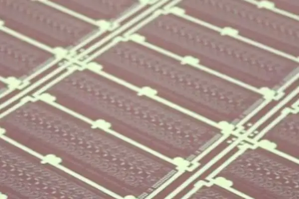
Industrial Automation PCB Reliability: How to Achieve 10+ Years of Stable Operation
In the field of industrial automation, people often pay attention to AI
Every time I see those complex circuit board designs, I recall the confusion I felt when I first entered this field. Back then, I always thought that as long as the circuit was connected, it would work well. Later, I realized that the world of high-frequency signals is completely different. I remember once debugging an RF module; all the components were soldered correctly, but the signal was still a mess. After struggling for several days, I realized the problem was with the circuit board’s impedance. This taught me a valuable lesson: with high-speed signals, a circuit board is no longer just a simple wire connection; it’s more like a sophisticated electromagnetic waveguide.
Impedance matching is actually quite interesting. Just as two people need to understand each other’s language to communicate, signal sources and loads also need to communicate using the same “language.” If the characteristic impedance of the circuit board is mismatched, the signal will reflect like sound waves bouncing back and forth in a room. This reflection not only weakens the energy of the effective signal but also adds various strange glitches and ringing to the waveform. I’ve seen too many cases where entire projects have been reworked because this issue was ignored.
Speaking of impedance control practice, I think the most important thing is to break free from the mindset of DC circuits. Many people are used to understanding impedance by measuring resistance with a multimeter, which is actually a misconception. Characteristic impedance is a dynamic electromagnetic parameter that depends on the geometry of the trace, the dielectric material, and even the operating frequency. For example, traces of the same width will exhibit completely different impedance characteristics on PCBs with different layers.
Now, when designing, I pay special attention to the layer stack-up. Sometimes, to achieve a specific impedance value, I’m willing to increase costs by choosing a higher-quality substrate. Because I know that spending a few hundred dollars more on materials upfront can save weeks of debugging time later. Especially when dealing with differential signals, even a 0.1mm difference in spacing between two traces can lead to severe common-mode noise.
The testing phase is often where problems are most exposed. I usually use simulation software for preliminary assessments before prototyping and testing to verify the design’s effectiveness.
Recently, while working on a 5G-related project, I encountered a new challenge: millimeter-wave circuit boards are extremely sensitive to surface roughness. This made me realize that as technology advances, we need to continuously update our understanding of impedance control.
Ultimately, the key to good impedance control is to consider every detail as part of the overall system. From material selection to routing rules to manufacturing processes, every step affects the final result. This requires designers to have interdisciplinary knowledge and rich practical experience.
When I first started designing high-speed circuits, I always thought that simply connecting signals was enough. Later, I realized that the science of routing is much deeper than I imagined.
I remember once debugging a board where the signal quality was consistently unsatisfactory. After much troubleshooting, I finally discovered that the trace width wasn’t properly controlled.
The dielectric constant of the board material used initially was unstable, resulting in significant performance differences between different batches.
Later, switching to specialized high-frequency materials improved the situation considerably.
Many people tend to overlook the impact of dielectric thickness on signal strength.
I’m accustomed to planning the paths of critical signals during the layout phase.
Sometimes, I see boards designed with inconsistent trace thickness; such routing makes it difficult to guarantee stable impedance characteristics.
Impedance matching isn’t simply a matter of calculation formulas; tolerance control during actual manufacturing is also crucial.
Once, testing revealed inconsistencies in the characteristics of boards from the same batch; investigation revealed that the lamination process caused fluctuations in the dielectric layer thickness.
Now, I pay special attention to leaving sufficient margin during design.
When selecting board material, one shouldn’t only look at the nominal parameters but also consider the actual application scenario.
For example, in high-frequency environments, the stability of the Dk value is more important than its absolute value.
Sometimes, pursuing ultimate performance necessitates accepting higher costs.
However, in most cases, choosing the right material is sufficient.
During routing, I try to keep critical signals away from interference sources.
I also pay attention to the coupling effects between different layers.
These details may seem insignificant, but their impact on overall performance is considerable.
Experience tells me that good design is often reflected in these subtle details.
Every time I test a prototype, my biggest expectation is to see the simulation results match the measured data.
This sense of accomplishment is probably the driving force behind my continued work in this field.
Every time I see those complex formulas for calculating impedance values, I find it a bit funny. When you’re actually building a board, you realize that theoretical discussions and actual production are completely different things. I’ve seen too many engineers spend all their time on simulation software while neglecting the most basic geometric issues.
I remember last year a client came to me complaining about his terrible signal quality. I looked at the board and immediately understood the problem—he thought that simply setting the trace width according to the textbook formulas would solve everything. In reality, in multilayer boards, the copper traces on adjacent layers can have unexpected effects on your routing, which cannot be solved simply by adjusting parameters.
The most troublesome aspect of impedance-controlled PCB design lies in those seemingly insignificant details. For example, the dielectric thickness of the same batch of boards can vary by several percentage points after lamination under different temperature and humidity conditions. Not to mention fluctuations in linewidth during etching; all of these can render your precise calculations meaningless.
Once, we tested boards from different manufacturers and found that the actual characteristics produced with the same design parameters could differ by up to 15%. That’s when you understand why veteran engineers always say you need to be in the factory and supervise production. Relying solely on software simulation? That only gives you an ideal value.
Many young people today rely too much on automation tools and neglect the most basic physical laws. Signal propagation in transmission lines follows electromagnetic field theory, which cannot be summarized by a few formulas. I often tell my team to understand the three-dimensional structure of a PCB like a sculptor treats clay, because every corner and every via changes the distribution of the electromagnetic field.
Speaking of vias, this is perhaps the most easily underestimated aspect. Many people think that drilling a hole can’t have much of an impact. But when you’re dealing with GHz-level signals, that small metal cylinder becomes the biggest variable. We conducted comparative tests, and optimizing the via design improved eye diagram quality by over 30%.
A recent project particularly struck me. The client insisted on pursuing extreme linewidths, claiming it was to save space, resulting in a disastrous yield. Often, relaxing the requirements slightly yields more stable performance. After all, engineering is the art of compromise, not a mathematical competition.
I most admire designers who understand balance. They don’t rigidly adhere to theory nor blindly experiment; instead, they treat each board as a unique work of art. No two boards have exactly the same characteristics, which is both the most fascinating aspect and the greatest challenge of this field.
Over the years of PCB design, I’ve gradually noticed an interesting phenomenon: many people, when faced with impedance control, rush to calculate formulas and adjust trace widths, yet the actual boards still suffer from numerous problems. The key often lies not in the calculations themselves, but in how you understand the variables throughout the manufacturing process.
I’ve encountered many cases where the design documents clearly indicated precise routing parameters, but the measured impedance deviation after lamination could exceed 10%. After talking with factory workers, I realized the problem stemmed from material deformation. For example, during multilayer board lamination, the fluidity of the prepreg can cause uneven dielectric thickness. Simply staring at the ideal model in the software is useless; you have to consider the fluctuations in actual production. For instance, during the lamination of an eight-layer board, the prepreg, under high temperature and pressure, can flow like syrup, causing a 3-5 micrometer reduction in dielectric thickness in localized areas. This tiny change is enough to cause a 2-3 ohm shift in characteristic impedance. Even more troublesome is the unpredictability of this flow, which is closely related to the temperature uniformity of the laminator and the pressure profile settings.
Once, while designing a high-speed backplane, we specifically optimized the reference plane of the impedance PCB. However, we discovered a detail we’d overlooked – the bridging capacitors at the power layer splits weren’t properly positioned, causing the return current to detour and introducing noise. This made me realize that impedance control isn’t just a matter of geometry; the integrity of the return current path is perhaps even more crucial, especially for high-frequency signals. Those invisible currents actually run beneath the reference plane. For example, when a signal line crosses a power layer split, if there aren’t enough decoupling capacitors within 200 mils of the crossing point, the return current will be forced to take a longer path. This extra loop not only increases the equivalent inductance but also radiates electromagnetic interference like an antenna.
Now, I always leave room for adjustments when planning layer stack-ups. For instance, while the symmetrical structure on both sides of the core board theoretically prevents warping, the stress distribution of the board after lamination will still have slight differences. Therefore, I need to confirm with the manufacturer beforehand the types of prepreg they commonly use. Some have high resin content and strong fluidity, making them prone to shrinkage after lamination, so more margin is needed. Specifically, we ask the factory to provide thickness fluctuation data for each type of prepreg in three lamination tests, and then select the model with the smallest standard deviation. For critical signal layers, we even intentionally set the target impedance to 48 ohms instead of 50 ohms during the design phase, leaving a 2-ohm tolerance margin for production.
Recently, while working on millimeter-wave projects, I’ve become even more aware of the problems caused by dispersion effects. The same 50-ohm trace can show a difference of several ohms in impedance measured at 5GHz and 30GHz. We later switched to PTFE substrate, which, although more expensive, offered significantly better stability. This made me realize that material selection shouldn’t be based solely on initial parameters but must be evaluated in conjunction with the frequency range. For example, the dielectric constant of ordinary FR-4 material changes from 4.3 to 4.0 at 10GHz, while PTFE material only changes from 2.2 to 2.17 within the same frequency band. This stable dielectric characteristic improves phase consistency by more than three times, making it particularly suitable for phase-sensitive applications like phased array antennas.
In fact, the most tedious aspect of impedance control is that it requires constant mutual calibration between the design and manufacturing stages. Sometimes the factory reports that a certain prepreg is out of stock and a substitute material needs to be used. This necessitates re-simulating the trace parameters. Although this process is tedious, it avoids batch problems later on and saves time. We’ve established a rapid material substitution evaluation process. When material changes occur, simply inputting key parameters such as the new material’s Dk/Df curve, resin content, and glass cloth type allows the simulation software to generate a revised linewidth scheme within half an hour, significantly shortening the verification cycle.
I increasingly believe that good impedance design isn’t about rigidly adhering to theoretical values, but rather understanding the trade-offs behind each decision. For example, whether to increase costs for symmetry or accept a slightly larger impedance tolerance to improve yield—there are no standard answers; it depends on the specific project’s requirements for signal integrity. Like the recent automotive radar project, although theoretically requiring an impedance tolerance of ±5%, considering the 15% yield drop during mass production, we ultimately negotiated with the client to widen the tolerance to ±7%. This adjustment reduced scrap by over two hundred per thousand boards, resulting in a 12% reduction in overall cost.
I’ve seen too many engineers overcomplicate impedance control. What’s truly important isn’t those fancy theoretical formulas—it’s the feel of the board after you’ve actually handled it.
I remember being incredibly nervous the first time I designed a high-speed PCB—terrified the signal wouldn’t transmit. But I discovered that as long as the transmission line width was calculated accurately, the PCB manufacturer could generally handle it. The key is knowing when to be meticulous and when to let go.
Many people associate impedance with expensive equipment for measurement—but in my daily projects, I focus more on prevention during the design phase—such as the rationality of the layer stack-up and whether the traces avoid sensitive areas. These details are often more important than later testing.
Once, a board I designed passed TDR testing, but experienced signal problems in actual use. It turned out the impedance matching at the connectors wasn’t handled properly. This lesson taught me that test data is only a reference; true stability needs to be considered from the perspective of the entire system.
Now, when designing impedance-sensitive PCBs, I pay special attention to easily overlooked details—such as the copper foil treatment around vias and the impact of surface treatment processes on the final impedance. These seemingly minor factors often determine success or failure.
Recently, I tried a new simulation method—predicting the impedance variation range after actual production during the layout phase. This is much more proactive than simply relying on later testing and gives me more confidence in the design results. Ultimately, good impedance control should be a mindset that permeates the entire design process—not just a final testing step. When you truly understand how signals behave in transmission lines, you’ll naturally know where to focus your efforts.
Sometimes I deliberately set up extreme cases on test strips to see how well the PCB manufacturer actually controls the impedance—this kind of practical experience is more valuable than any theory.
Ultimately, every project is unique—there are no universally applicable rules—the important thing is to maintain an open mind and continuously adjust your understanding and methods in practice.
Having done PCB design for so many years, I’ve noticed a rather interesting phenomenon. Many people find impedance control PCBs incredibly mysterious, as if you need to master some profound theory to even attempt it. It’s not that complicated; the key is to view design and manufacturing as a whole. I remember a project where I failed because of this; I made the impedance simulation curves in the software look perfect, but the PCB manufacturer couldn’t reproduce them.
That lesson taught me that the ideal model in simulation tools and the actual manufacturing process in the factory are completely different things. For example, even with the same material parameters, the dielectric constant of substrates from different batches can differ by several percent. Not to mention the fluctuations in etching precision and lamination alignment during processing. Later, I learned my lesson and now always talk to the PCB manufacturer’s engineers about the actual capabilities of their production lines before designing impedance PCBs.
Now, I pay special attention to this aspect when designing high-frequency circuits. Sometimes, to match specific impedance values, I’d rather slightly widen the trace width to leave room for manufacturing. After all, even the most perfect simulation results are useless if they can’t be replicated. A recent millimeter-wave project was like this; during the simulation phase, we anticipated sudden impedance changes at certain microstrip line corners and adjusted the routing topology in advance.
Actually, I think impedance control is most challenging in terms of attention to detail. For example, if a board has both single-ended 50-ohm and differential 100-ohm impedances, you need to consider the stack-up structure and routing space comprehensively. Once, to balance the impedance matching of two high-speed buses, we cleverly created a notch in the power layer to solve the crosstalk problem.
Speaking of which, I must mention the significant advancements in EDA tools. Previously, we had to manually calculate the width and spacing of microstrip lines; now, importing the PCB manufacturer’s process parameters allows for automatic optimization. However, even the most intelligent tools cannot replace the engineer’s experience and judgment, especially when dealing with the unseen electromagnetic field effects in RF circuits.
I recently experienced this firsthand while working on a 5G base station project. Although the simulation software provided the theoretically optimal solution, during actual debugging, I found that the return loss in certain frequency bands was consistently unsatisfactory. Eventually, I solved the problem by adjusting the position of the grounding via by half a millimeter based on my intuition about transmission line theory. Such subtle adjustments are often more effective than rigidly adhering to simulation data.
Ultimately, impedance control is like walking a tightrope; it requires finding a balance between ideal design and actual manufacturing processes. Sometimes, when I see young engineers frowning at simulation reports, I suggest they spend more time in the production line. Seeing firsthand how immersion gold wires are formed in the etching solution provides a completely different understanding of impedance deviations.
I firmly believe that good PCB design should be like cooking: it requires a precise recipe but also the ability to adjust the heat according to the stove’s flame. Those seasoned engineers who can control impedance deviation within 5% are often not the most knowledgeable about electromagnetic fields, but rather those with the deepest understanding of material properties and manufacturing processes. This is perhaps the essence of engineering art.
I’ve recently been pondering something quite interesting—the delicate balance game in PCB manufacturing, especially when you need to precisely control signal transmission quality.
I remember once testing a prototype and finding signal integrity issues. Later, I realized it was due to uneven copper thickness. The plating process for the outer layers requires particular attention to consistency.
Sometimes, looking at the acid-corroded edges of the traces makes me think a lot. This stage really tests your craftsmanship.
What I find truly interesting is the interaction of various factors throughout the process.
Once, we tried comparing substrates from different suppliers. The results showed that, with the same design parameters, the measured values could differ by more than ten percent.
Speaking of impedance PCB manufacturing, I think the most easily overlooked aspect is the consistency of material properties.
I’ve seen many engineers focus solely on parameter settings in the design software, neglecting the variables in actual production.
In fact, with more experience, you’ll find that good circuit board manufacturing is more of an art than simply a technical skill. You need to understand the interrelationships between each step. For example, how does temperature and pressure during lamination affect dielectric thickness? How does current density during electroplating affect copper uniformity? And that seemingly simple pattern transfer process actually hides a lot of knowledge.
Now, whenever I see high-frequency circuit boards in precision instruments, I pay special attention to their layered structure and the smoothness of the line edges. These details often determine the upper limit of the entire board’s performance.
I’ve always felt that many people overcomplicate PCB design. Essentially, a circuit board is about paving the way for electronic signals—you have to ensure the signals can run smoothly.
When I first started working with high-speed circuits, I also made mistakes. Once, I designed a USB interface board, but the computer wouldn’t recognize it. After much troubleshooting, I discovered that the differential line spacing wasn’t properly controlled, causing signal interference. I had to readjust the routing to solve the problem.
Many people get a headache when they hear about impedance control, but it’s not as mysterious as it seems. The key is to understand the characteristics of current. Like water, it reflects when it encounters a sudden narrowing or bend, so we need to maintain the continuity of the path.
Many engineers often overlook the mutual influence between different signal lines, especially when they are close together. This coupling effect can make an otherwise stable signal unreliable. Sometimes, even if the characteristics of individual lines meet the requirements, the overall performance degrades when they are routed side-by-side.
I like to use highway construction as an analogy for PCB design. You need to ensure each lane is smooth and that the medians between different lanes are neither too close nor too far apart, so that vehicles can pass efficiently without interfering with each other.
Recently, I encountered a similar problem while modifying an RF module for a friend. The two antenna feed lines were too close together. Although the characteristics of the individual lines met the requirements, the signal quality was significantly reduced during actual testing. The problem was solved only after the spacing was increased to three times the line width, which made me realize the importance of spatial layout again.
Ultimately, good PCB design is not about obsessively working with a single parameter, but about ensuring the entire system coexists harmoniously. Sometimes, slightly adjusting the routing or changing the layer stack-up can be more important than simply pursuing a certain value. After all, circuits are dynamic, not just theoretical numbers.
Over the years of PCB design, I’ve found that many people’s understanding of impedance control remains at a superficial level. People often focus on trace width and spacing, but frequently overlook a more fundamental factor: board thickness. In fact, thickness is the most easily overlooked key factor; it’s like the foundation, directly affecting the stability of the entire signal.
I’ve seen many projects where thickness deviations led to signal quality degradation. Once, while working on a high-speed interface board, we encountered severe signal reflection. After much investigation, we discovered that the dielectric layer thickness of the board material supplied was 8% thinner than the nominal value. Although the traces were routed strictly according to design specifications, the actual impedance value deviated from the target value by nearly 6 ohms. This deviation might not be noticeable in low-speed circuits, but under GHz-level high-speed signals, it can cause severe inter-symbol interference and eye diagram closure. Especially when multiple signal lines have impedance mismatches simultaneously, the bit error rate of the entire system increases exponentially.
Now, when designing impedance PCBs, I always prioritize thickness tolerance. Slight differences between boards from different manufacturers, and even between different batches from the same manufacturer, can affect the final impedance accuracy. Instead of relying entirely on calculation formulas, it’s better to allow for adjustments during the actual prototyping process. For example, during early simulations, a thickness fluctuation range of ±10% is preset, and the most robust design solution is found through parameter scanning analysis. Impedance-sensitive areas are also specifically marked in the Gerber file, requiring the PCB manufacturer to strengthen thickness control in these areas.
Truly reliable impedance control PCBs should involve intervention from the material selection stage. I request detailed board parameter reports from manufacturers, especially the actual thickness data for each batch of materials. Sometimes, to achieve more precise impedance matching, I’m even willing to accept slightly higher costs by using specialty materials with smaller tolerances. After all, for high-speed circuits, signal integrity is far more important than saving a little money. High-frequency materials like Rogers 4350B, although more expensive, have thickness tolerances that can be controlled within ±3%, making them particularly suitable for array antennas or multi-channel acquisition systems with strict impedance consistency requirements.
In actual layout, I prefer to place critical signal lines on the same layer to maintain reference plane consistency. I’ve encountered designers who, for routing convenience, split differential pairs onto different layers, resulting in phase deviations due to differences in interlayer dielectric thickness. This problem is particularly difficult to detect during debugging and often only surfaces during system-level testing. For example, during the debugging of a 28Gbps SerDes link, it was discovered that because a pair of differential lines were routed on L2 and L4 layers respectively, even with well-matched line lengths, the difference in dielectric thickness between the two layers resulted in a 0.3ps delay difference, ultimately requiring a redesign to resolve.
This point was further validated recently while working on a batch of RF boards. We specifically compared two substrate materials of different thicknesses and found that even using the same routing scheme, the measured impedance values showed significant differences. This further convinced me that in high-speed, high-frequency design, substrate thickness must be considered an active design parameter rather than a passive manufacturing condition. Especially in the microwave band, variations in dielectric thickness directly affect the effective dielectric constant, thus altering the electromagnetic wave propagation speed. This necessitates incorporating thickness variables into the impedance model’s correction coefficients during the design phase.
Ultimately, good impedance control isn’t based on some magical calculation formula or software tool, but rather on a deep understanding of material properties. Every time I see designs that only focus on trace width while ignoring thickness control, I feel like I’m ignoring the bottom block when building with blocks. Perhaps this is why some boards, despite having perfect design parameters, always fall short in actual performance.
I think the most interesting thing about this industry is that you can always learn something new from failures. Those impedance issues that used to give me headaches have now become my most valuable experience. Every project reminds me to look at signal integrity issues from a more comprehensive perspective. For example, when evaluating a new project now, I consider at least a dozen material parameters simultaneously, such as dielectric thickness, copper foil roughness, and fiberglass effects. The accumulation of these details ultimately determines the performance limits of the product.
In the field of industrial automation, people often pay attention to AI
Ever wonder how your phone maintains a stable signal? It relies on
When selecting components for a security monitoring system, most attention goes to
- خبير في إنتاج دفعات صغيرة إلى متوسطة الحجم
- تصنيع ثنائي الفينيل متعدد الكلور عالي الدقة والتجميع الآلي
- شريك موثوق لمشاريع تصنيع المعدات الأصلية/التصنيع عند الطلب الإلكتروني
ساعات العمل: (من الإثنين إلى السبت) من الساعة 9:00 إلى الساعة 18:30