

What Documents Are Required for PCB Production: A Field Guide From Real Industrial Weighing Controller PCB Projects
Many engineers focus too much on technical parameters early on and overlook
Every time I see the blinking signal light on the humble router box at home, I always think that most people may not realize how much the thin circuit boards inside carry. We always discuss how wide the Wi-Fi signal coverage is and how fast the network speed is, but we seldom care about where these experiences come from. In fact, the answer lies in that small PCBA.
I have been involved in the disassembly of many routers and found an interesting phenomenon: many manufacturers like to make the heat sinks extremely exaggerated, and the casing is designed to be very technological, but the things that really determine the performance are often hidden underneath. A good multi-layer PCB design has far more value than simply connecting components. It is more like a carefully planned urban transportation system. Data packets are vehicles. How to send them to the right place in the shortest time while avoiding congestion and interference requires extremely high design wisdom. For example, engineers need to use simulation software to repeatedly optimize wiring to ensure that high-speed signal paths are as short and straight as possible, and to set isolation zones for signals of different frequencies to prevent crosstalk.
Take the current Wi-Fi 6E and the new standards that are about to become popular, the processing of high-frequency signals has become extremely sensitive. I remember one time when I was testing a high-end router, I found that if the length of an antenna trace on the PCB was just a few tenths of a millimeter off, the signal strength dropped by nearly 15%. This may sound trivial, but in practice it means that watching videos through a wall may stutter. So those who think that the internal designs of routers are similar are actually quite naive. This is because the wavelength of high-frequency signals is extremely short, and the physical length of the trace will directly affect the phase and impedance matching of the signal. The mismatch will cause signal energy reflection instead of effective radiation.
Nowadays, many people pay too much attention to the brand specifications of components when assembling PCBA, but ignore the quality of the substrate itself. I have seen some cases where low-quality boards were used to reduce costs. The initial test may be fine, but after the first half a year of use, various inexplicable disconnection problems will occur. In high-temperature and high-humidity environments, the stability of the plate directly affects the life of the entire machine. This is like building a house without paying attention to the foundation. No matter how beautiful the appearance is, it cannot withstand the test of time.
Inferior boards have high dielectric loss and large thermal expansion coefficient. After long-term use, the electrical performance will be seriously degraded, resulting in a decrease in signal integrity.
The design of the radio frequency part is a test of the engineers’ skills. Many people think that the more antennas, the better the signal. In fact, if the RF trace layout on the PCB is unreasonable, mutual interference between antennas will reduce efficiency. Good design will allow each antenna to do its job, working together instead of fighting each other. This requires a lot of simulation testing and experience accumulation. For example, in MU-MIMO technology, the signal phase relationship between multiple antennas must be precisely controlled to form an effective directional beam.
I always believe that the value of a router should not only be reflected in the gorgeous numbers on the parameter sheet. The real user experience comes from a stable and smooth network connection, which is inseparable from the support of each carefully designed circuit board. Next time you complain about unstable network, maybe you can first think about whether it’s time to change to a device with more solid internal workmanship.
Supply chain choices are also becoming increasingly critical. Many manufacturers are now promoting local substitution, which is a good thing in itself, but how to ensure that quality does not decline in the process is a challenge. Some domestic multi-layer PCB boards are already close to international standards in performance, but there is still room for improvement in performance in some extreme environments. This requires the joint efforts of the entire industry chain. For example, high-frequency and high-speed plates rely on special resin systems and glass cloth weaving processes. The research and development and production processes of these core materials still need to continue to be tackled.
After all, the router, a seemingly simple device, actually reflects the improvement of the entire electronics manufacturing industry. From single panels to complex multi-layer PCBs, from simple wired connections to today’s complex wireless Mesh network support, every technological advancement is inseparable from the innovation of the underlying hardware. When we enjoy the convenience brought by high-speed Internet, perhaps we should also give some applause to those unknown hardware engineers.
After all, in this era of interconnected everything, that circuit board hidden in a plastic shell is connecting the entire world in a way that we cannot see.
I have always felt that many people’s understanding of routers is still at the stage of “just being able to access the Internet”. This thing is actually quite interesting. Think about it, we hold our mobile phones every day to watch videos and play games, and all the data must first pass through that inconspicuous little box. The circuit board inside it, that is, the Router PCB Assembly, is the key to whether your network experience is smooth or stuck like a PPT.
When I was doing product design in the early years, I was exposed to many solutions. At that time, everyone thought that just adding more functions would be enough. As a result, the machine became very hot and the signal was unstable. Later, I slowly understood that the real test of skill is often not how many new chips are used, but whether the basic design can keep up. For example, many high-end routers now use Multilayer PCB. It’s not just about sounding superior. Multilayer boards can better plan signal wiring paths, separate high-speed signals, power supply and control signals, greatly reducing mutual interference.
Speaking of interference, this is the most troublesome part of the Wi-Fi experience. I’ve encountered this before at home. The signal is obviously full, but the Internet speed just can’t go up. After further investigation, I discovered that there was a wireless charger placed next to the router. In today’s home environment, there are too many wireless devices of all kinds, from Bluetooth headsets to smart home appliances, all crowded in the limited frequency band. In addition to these devices that actively transmit signals, microwave ovens, refrigerator compressors, and even some low-quality LED light driving power supplies may produce electromagnetic noise during operation, which can pollute the wireless environment like background noise. To further complicate matters, the reinforced concrete walls of modern residences also have strong attenuation and reflection effects on signals, which may lead to multipath interference, that is, the same signal reaches the receiving end through different paths and at different times, causing signal distortion. Therefore, an excellent router design must have built-in powerful anti-interference algorithms and intelligent signal processing units that can dynamically identify and avoid congested channels, or use beamforming technology to accurately focus signal energy in the direction of the device instead of spreading it evenly around.
So you see, simply increasing the antenna power or claiming to support the latest Wi-Fi 7 protocol sometimes does not solve the fundamental problem. The key lies in the collaborative design capabilities of the entire system. A well-designed circuit board is like a seasoned traffic commander, knowing when to let data packets pass through which channel quickly. For example, when processing low-latency data streams from game consoles and high-bandwidth video streams from smart TVs, it requires intelligent traffic identification and priority scheduling (QoS). This requires extremely low-latency, high-bandwidth interconnection between the network processor, memory, RF front-end module and power supply system on the PCB. Bottlenecks in any link will become the shortcomings of the barrel. Excellent layout and routing can ensure the shortest and cleanest critical signal paths, while sophisticated power management design can provide pure and stable voltages for different modules to prevent abnormal chip operation or performance fluctuations caused by voltage fluctuations.
I have seen some products push the chip frequency very high in order to pursue the ultimate speed parameters. As a result, the heat dissipation is not done well, and the chip overheats and reduces the frequency after a while. This is as unrealistic as asking a sprinter to run a marathon without giving him water to drink. Efficient heat dissipation design is not just about adding a piece of metal or opening a few holes. It involves precise analysis of the distribution of the chip’s heat source and designing the heat conduction path accordingly. Some designs use special PCB materials with high thermal conductivity (such as metal substrates or ceramic substrates), or arrange a large array of vias under key chips to quickly conduct heat to the heat sink on the back. Active cooling by fans requires a balance between air ducts, noise and dust prevention. Without good thermal management, the chip will not only reduce frequency under high temperatures, but its long-term reliability and signal integrity will also be greatly reduced, and the bit error rate will increase, ultimately affecting the user experience.
Good design should be an art of balance with trade-offs. Engineers need to find the sweet spot between cost, performance, power consumption, heat dissipation, size and even aesthetics.
Blindly stacking high-end components without considering system matching often results in half the effort.
In the final analysis, users don’t actually care how many layers of circuit boards you use or which generation of Wi-Fi protocols you support. They only care about whether the actual experience is smooth and stable, with no delays and no drops. This is the ultimate goal that all technologies must serve.
I have always felt that many people’s understanding of routers is still at the stage of “just being able to access the Internet”, which is actually quite a pity. Recently, I have toyed with a few boards and found that the doorway here is much deeper than we thought. Take the most basic PCB as an example. Many people may not know that better home routers now use Multilayer PCB. Four and six layers are the norm, and some high-end models even have eight layers. Why do you need so many layers? Because there are too many signal channels, you have to separate the power layer, ground layer and various signal lines. Otherwise, those high-speed data streams will fight in the board. Do you still expect it to be stable?
Speaking of stability, we have to mention radio frequency. This is where design skills are truly tested. We always complain that the signal is weak through walls and drops frequently. In fact, many times the problem is not with the antenna, but with the tiny circuits on the board responsible for radio frequency processing that are not tuned properly. A small chip is surrounded by capacitors and inductors. If their placement differs by a few tenths of a millimeter, the performance may be greatly compromised. I have seen some boards with rough designs that placed the radio frequency part and the digital part too close to each other in order to save costs. As a result, the noise from the digital circuit directly passed through and interfered with the wireless signal. For example, switching noise generated by a poorly designed DC-DC converter, if coupled into a sensitive RF receive path, will directly raise the noise floor of the receiver, causing a sharp decline in connection quality over long distances or with weak signals. This kind of interference is particularly obvious in the 2.4GHz frequency band, because this frequency band is already crowded, and internal noise will make the router more susceptible to frequency interference from external microwave ovens, Bluetooth devices, etc.
This also leads to the key of Router PCB Assembly. Today’s assembly is no longer just about soldering the components on. Especially when you want to stuff 10 Gigabit network or the latest Wi-Fi standard into that small box, you have to be careful every step of the way. Is the placement machine accurate enough? Is the reflow soldering temperature profile set correctly? Have you done an X-ray to see if the solder joints hidden under the chip are welded or bridged? These details are invisible to ordinary users, but they determine whether the device in your hand is “industrial art” or “electronic waste.” Taking reflow soldering as an example, lead-free solder requires a higher peak temperature, but improper control of the temperature rise slope can easily lead to excessive thermal stress inside the chip or blistering and delamination of the PCB board, posing hidden dangers for long-term use.
The chip selection is even more interesting. In the past, everyone always thought that the solutions from major foreign manufacturers were reliable and stable, but now the situation is really different. I have come into contact with some domestic chip solutions and found that they are more thoughtful in terms of integration and power consumption control.
Of course, this does not mean that there are no challenges. New chips often mean new packaging forms. For example, some domestic controllers like to use more compact LGA packaging, which has completely different requirements for PCB pad design and assembly process. You have to relearn how to deal with it. The LGA package has no exposed pins, and its connection relies entirely on the alignment and welding of the array pads on the bottom of the chip with the pads on the PCB. This imposes almost stringent requirements on the coplanarity of the PCB, the flatness of the pad surface treatment (such as ENIG), and the accuracy of solder paste printing. Any slight deviation may lead to connection failure.
So I think we need to look at products like routers from a different angle. It is no longer a simple “network repeater”, but a complex system that integrates high-speed digital design, analog radio frequency technology and precision manufacturing processes. The next time you see a new router advertising 10 Gigabit ports and multiple frequency bands, you might as well think about how high frequencies this means the traces on the PCB have to withstand, and how many signal integrity problems the engineers responsible for assembly have to overcome. Once you understand these things and then look at the parameters, you will find that many of the “highlights” in the promotion are actually the technical thresholds taken for granted, and some unmentioned details, such as the materials used for the internal panels or the level of the assembly foundry, may be the key to truly determining whether it is useful or not. For example, the dielectric constant stability of the board directly affects the loss and phase consistency of high-speed signals, and an experienced foundry can control indicators such as patch offset and solder joint void rate to very low levels through strict process control. These are the cornerstones of long-term stable operation of equipment in high-temperature and high-humidity environments.
I have always felt that many people’s understanding of routers is too one-sided. Everyone always looks at the number of antennas or the nominal speed. In fact, it is the basis that determines whether a piece of equipment can stably run at full speed and how effective it is at penetrating walls. It’s exactly the circuit board hidden in the case that no one will take a second look at.
Take, for example, an enterprise-grade device I recently took apart. Its motherboard uses an eight-layer design. This is not stacking for the sake of stacking. The arrangement of each floor is exquisite. The outer two layers handle high-speed interface signals such as SFP optical ports or 10 Gigabit electrical ports. They need the shortest and cleanest path to enter the main chip, with a complete ground plane and power plane sandwiched in the middle. This is like building a soundproof wall on the highway, which can effectively shield the switching noise of the digital circuit itself. The innermost layer of wiring is reserved for relatively low-speed but large number of control signals, such as the status indicators of each LAN port and the control lines of the USB interface. The idea of layered isolation is to allow signals of different natures to go their own way without interfering with each other.
Speaking of this, I have to mention that the welding process of optical module interfaces such as SFP is a relatively delicate part of the Router PCB Assembly.
The metal casing of that interface must be tightly attached to the pads on the motherboard. This is not only for physical fixation, but more importantly, the casing is grounded. If it is soldered falsely, the shielding effect will be greatly reduced. External electromagnetic interference can easily penetrate through here and affect the pair of extremely delicate high-speed differential signal lines inside. As a result, the network intermittent speed cannot be increased.
So if you look at a good multi-layer board, it provides a systematic guarantee to reduce the probability of problems occurring at the root.
I have seen some designs that were supposed to use six-layer boards and stuffed them into four-layer boards in order to reduce costs. The result is that the power traces and data signal lines are squeezed into the same layer and very close to each other. High-frequency changing currents on the data lines will introduce ripples on the power network, leading to unstable power supply. The performance of the main chip will fluctuate, and the performance of the main chip will fluctuate. When playing games, the ping value suddenly spikes and you can’t find the reason.
The selection of materials is also very interesting. Now many high-end routers are beginning to use lower-loss boards. This kind of board has better performance at high frequencies and less signal energy loss. Of course, it is also more expensive, but for devices that pursue ultimate wireless performance, the investment is worthwhile. It is directly related to whether your phone can still play 4K videos smoothly after being separated by two walls.
After all, the design of a router is very similar to when we build a house. The foundation and main frame are solid. Only the decoration behind it is meaningful. A well-designed multi-layer PCB is the foundation, which determines the ceiling of the performance of this device. As for those cool functions and gorgeous software interfaces, they are all built on this solid foundation. If you put the cart before the horse, the experience will definitely not be better.
I think many people now have misunderstandings about router design. They always think that stacking materials can produce good products. In fact, what really affects the experience are often the invisible details, such as the selection and processing of PCB boards.
I have seen many manufacturers still using ordinary FR4 boards to make high-end routing motherboards in order to control costs. This is like using ordinary water pipes to transport high-pressure water flow. The signal loss is particularly large during the transmission process. Especially when dealing with high-frequency signals such as Wi-Fi 7, the problem will be more obvious. Users may think that the parameters of the router are very beautiful, but in actual use, the speed will drop across the wall.
The design idea of multi-layer PCB is actually quite interesting. In the past, people thought that the more layers, the better the heat dissipation. In fact, increasing the number of layers is to provide a clean loop path for signals. If the traces of the radio frequency part are crowded together with the digital part, mutual interference will be serious. Sometimes the antenna configuration is good but the stable signal cannot be received. This is the reason.
I prefer the design idea of treating different functional areas separately. For example, the RF part is placed separately on a low-loss board for sub-board processing and then connected to the main board. Although this will increase the complexity of Router PCB Assembly, the effect is indeed different.
When choosing a plate, don’t just look at the numbers on the parameter table. Some materials have very good nominal low-loss properties, but their performance will drop a lot under the actual operating temperature. Especially those placed in weak current boxes with poor heat dissipation will have problems with their long-term operation stability.
A truly good design should take into account the balance of the entire system rather than simply pursuing the ultimate in a certain indicator. For example, if you use top-notch low-loss materials, but if the power supply part is not designed well and generates a lot of noise, then no matter how good the radio frequency performance is, you will not be able to achieve it.
I feel that many product promotions nowadays focus too much on surface parameters and ignore these basic engineering issues. When users buy it back and find that the actual experience is inconsistent with the propaganda, they can only blame it on “poor signal.” In fact, many times the problem lies in these invisible places.
The application of multi-layer PCB is not only to increase wiring density, but more importantly, to provide better shielding and isolation capabilities, which can isolate sensitive radio frequency circuits from noisy digital circuits to reduce mutual interference.
Sometimes I wonder why the actual performance of different brands of routers with the same configuration is so different. Maybe it’s because of the different investments in these basic processes. Those seemingly inconspicuous details often determine the final quality of the product.
A good design should allow each part to perform as it should rather than holding each other back. This requires engineers to have a deep understanding of each link rather than simply piecing together various high-end components.
After all, products are for people to use, not for benchmarking. Designs that focus on basic materials may not appear in a conspicuous position on the promotional page, but they do allow users to feel real stability in daily use.
When I was thinking about router PCB design recently, I found that many people think about it too complicated. In fact, the most important thing about Router PCB Assembly is often not the advanced theories, but whether you are willing to spend time to lay a solid foundation. I have seen many engineers struggle with how to stack Multilayer PCB so that it is advanced and how to route it so that it looks cool. As a result, they did not even understand the most basic signal path.
You have to first figure out how the signal runs instead of rushing to draw those complicated traces. Sometimes we pay too much attention to the so-called “best practices” but ignore the actual working environment of the equipment. For example, I worked on a project where the customer required the router to operate stably in a high temperature and high humidity environment. At this time, if you apply the equal length rules in the textbook, it may not be very effective because the characteristics of the material itself have changed. For example, the dielectric constant of FR-4 boards will drift with temperature and humidity, which directly affects the signal propagation speed. At this time, mechanical structure sealing and local heat dissipation design may take precedence over simply following wiring rules.
I always feel that current design relies a little too much on software simulation. Of course, simulation tools are useful, but you can’t completely trust it. Once I laid out a key trace perfectly according to the simulation results, but the signal quality actually declined during the actual test. Later, I discovered that an inconspicuous power module nearby was causing trouble. Its switching frequency happened to resonate with my signal. This problem was not reflected in the simulation model at all. This reminds us that it is crucial to establish an accurate device model and surrounding environment model before simulation, especially because the noise characteristics of the power supply are often simplified.
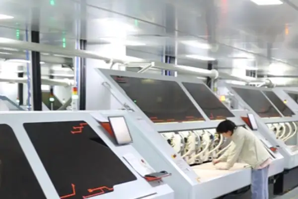
When it comes to the design of multi-layer boards, many people like to pursue more layers, as if the more layers, the better the performance. Actually that’s not the case. With more layers, the cost goes up and the processing becomes more difficult, which may not bring substantial improvement. I tend to use as simple a structure as possible while still meeting performance requirements. For example, sometimes a well-planned four-layer board is more effective than a casually drawn six-layer board. The key is that you have to understand what role each layer plays instead of blindly stacking them. Proper stackup planning, such as ensuring that each signal layer has an adjacent reference plane, can control impedance and crosstalk far better than simply increasing the number of layers.
Another point I think is very important is not to think of the router as an isolated device and design it to work in conjunction with the entire network environment. No matter how good your PCB layout is, if the antenna matching is not done well or the heat dissipation is not considered carefully, the performance of the entire system will still be greatly reduced. This may not have much to do with whether the traces are of equal length. Antenna location and clearance area design will affect wireless coverage, while poor heat dissipation paths may cause thermal underclocking of the chip. These system-level issues need to be taken into consideration in the layout from the beginning.
I feel more and more that good design is an art of balance. While pursuing signal integrity, you also have to consider manufacturability, cost and reliability. These factors are often mutually restrictive and it is difficult to have a perfect solution. So when I do design now, I will pay more attention to the overall coordination rather than the ultimate optimization of a certain part. After all, routers are meant to be used, not works of art to be appreciated.
In the final analysis, experience is more important than theory in PCB design. You have to do more trial and error to find a method that really suits you. Other people’s experience can be used as a reference but cannot be copied because the specific situations faced by each project are different.
By the way, one more thing I would like to remind everyone is not to be too superstitious about the so-called “high-end” process technology. Sometimes the simplest solution is the most reliable and economical. This is especially important when making consumer products because cost control is often more critical than a performance improvement of a few percentage points. Of course, the premise is that the basic performance must meet the standards. For example, when meeting shielding requirements, choosing a stamped metal shield may be more cost-effective than using a more expensive immersion gold process or special substrate.
I think the most interesting thing about this industry is that you can always encounter new challenges and always have new things to learn. This is probably what attracts me. Although it can be a headache sometimes, the sense of accomplishment after solving the problem is also real.
So if you are doing a similar design, my suggestion is to think more from the perspective of practical applications instead of just focusing on technical indicators. After all, what end users care about is not how beautiful your wiring is, but whether the router can access the Internet stably and quickly.
I recently discovered an interesting phenomenon when chatting with some friends who are engaged in hardware design: many people think that products such as routers are very mature, don’t they just put various chips on the board and solder them and that’s it? In fact, it is not that simple.
Take the most basic PCB as an example. Nowadays, slightly better routers basically use Multilayer PCB. Four, six, or even eight layers of PCB are very common. This is not to appear advanced, but signal integrity and power distribution really require so many layers to ensure. If you think about it, high-speed signal lines must be traced, impedance must be controlled, the power plane must be clean, and multilayer boards are almost the only option.
When it comes to welding technology, many people may still stick to the old concept and think that through-hole plug-ins are the most reliable. In fact, SMT technology is now very mature and most components are surface-mounted. However, there are indeed some places where through-holes are still needed, such as some connectors that need to withstand mechanical stress or high-power devices. At this time, you have to consider how to arrange the welding sequence.
I have experienced a project myself. In order to save trouble, I mixed through-hole components and surface-mount components for reflow soldering. As a result, several plastic connectors were directly deformed. Later, I realized that I had to do surface-mount reflow soldering first and then process the through-hole parts. Either use selective wave soldering or manual repair soldering. Although it was an extra process, the yield rate increased immediately.
In fact, reflow soldering itself is also a technical job. It is not just a matter of throwing the board into the furnace. Different boards, different components, and even different weather conditions have to adjust the temperature curve. I have seen some factories using a common curve to solder all the boards in a hurry. As a result, some small package capacitors and resistors were erected or moved under the large-size BGA chip, but instead were soldered. This kind of problem may not be detected in the short term, and the problem will gradually be exposed after a few months.
Wave soldering is used less now, but it is still irreplaceable in some specific scenarios. For example, manual soldering of through-hole connectors with particularly large numbers of pins is simply impractical. Wave soldering has to be relied on to control quality. There are many ways to control the quality. There is also a lot of flux, preheating time, soldering temperature, and every parameter must be adjusted correctly. Otherwise, the tin will not be connected or the soldering will be missed.
I always feel that making hardware is a bit like cooking. The same ingredients are used by different chefs, but the taste is different. The same is true for Router PCB Assembly. The reliability of the same design and different factories may be very different. The difference lies in these process details.
Many people may not realize that the quality of these welding processes directly affects how long the product can be used. I have dismantled some routers that have been used for two or three years and found that some solder joints have begun to turn black and even have small cracks. This is a potential failure point caused by the failure to control the welding temperature or time at that time.
So now when I look at a hardware design, I not only look at whether the schematic is beautiful, but also whether it can achieve those cool-looking high-density designs in production. If the factory’s process level cannot keep up, it will probably end up with a bunch of waste boards.
Good design should find a balance between performance and manufacturability. Knowing when to use multi-layer boards, when to stick to through-holes, and when to boldly use full surface-mount designs requires experience and continuous trial and error and learning.
After all, hardware is something that cannot be carelessly taken care of. Every detail may become a problem in the future. What we do is to build a bridge between design and production so that good ideas can truly be turned into reliable products. This is probably the most interesting part of this job.
I recently discovered an interesting phenomenon: many people always like to equate process complexity with quality level when discussing PCB manufacturing. It seems that if you use multi-layer boards or do a full set of tests, you will definitely be able to make a good product. In fact, it’s not that simple.
Take the router for example. Nowadays, many home routers on the market have begun to use Multilayer PCB in order to pursue signal strength and stability. With more layers, wiring is indeed easier and signal interference is reduced, but problems also arise – heat dissipation becomes particularly uneven. I have seen many cases where the temperature in some areas is too high and other areas are too cold because the heat distribution was not considered during the design. As a result, the BGA package has a weak solder or the small resistor is directly burned out. For example, some designs lay out high-power CPUs and radio frequency chips too closely without planning effective heat dissipation vias or heat conduction paths inside the PCB. Heat accumulates locally and cannot be dissipated quickly. Under long-term operation, component performance will accelerate decline, and even cause intermittent interruptions and other faults.
When it comes to welding processes, many people’s first reaction is wave soldering, which they think is the most mature and reliable process. Indeed, for traditional plug-in components such as power interfaces or large capacitors, wave soldering has high efficiency, low cost and good results. But now that the design of routers is becoming more and more compact, the component density is getting higher and higher, and traditional wave soldering is prone to problems – those precision chips that have been attached may be damaged by secondary heating. During the wave soldering process, the entire board needs to pass through a high-temperature molten tin furnace. For BGA, QFN and other packages that have completed reflow soldering, this is tantamount to an unnecessary thermal shock, which may destroy the stability of its internal structure or cause the alloy composition of the solder joint to change.
Therefore, more and more factories are now beginning to use selective welding technology to only perform local welding where needed. This can not only ensure the firmness of the plug-in components but also protect the surrounding precision components. This process uses precise programming to control micro-soldering nozzles to achieve precise point-to-point welding, completely avoiding secondary thermal effects on sensitive areas.
Regarding quality standards, I think many people have a one-sided understanding of IPC Class. Everyone always thinks that the higher the Class level, the better the product. In fact, it all depends on the actual use of the product. For example, there is no need for ordinary home routers to pursue Class3 standards because that means higher costs and longer production cycles, but the improvement to user experience may be minimal. The Class3 standard is usually aimed at military, aerospace or life medical equipment with high reliability requirements. It has extremely low tolerance for defects and requires near-perfect workmanship. While household electronic products are in a relatively mild environment, overly stringent standards will drive up unnecessary costs due to excessive inspection and extremely low throughput rates.
In most cases, the Class 2 standard is sufficient to meet the reliability requirements of the router. The key is to strictly implement it rather than blindly pursue a higher level. This means that every parameter in the production process, such as the thickness of the solder paste, the temperature profile of the reflow soldering, and the accuracy of the patch, must be stably controlled within the window allowed by the Class2 specification, and a traceable record must be formed.
The same is true for the testing process. The more equipment, the more reliable it is. SPI checks solder paste printing, AOI looks at mounting quality, X-Ray checks hidden soldering problems. These are all important, but more importantly, how to interpret these data and actually use them for production improvement. For example, SPI detects that the amount of solder paste is generally low, which may be due to improper design of the stencil openings, changes in solder paste viscosity, or drift in printer parameters. Only by in-depth analysis of root causes and adjustment of process parameters can inspection data be valuable.
I’ve seen some factories buy a bunch of high-end testing equipment, but the operators don’t know how to analyze the data. As a result, problems still occur and the yield rate still fails to improve. The equipment alarms and the operator simply passes the board or rejects it without correlating the defect image, location and process parameters for statistical process control (SPC) analysis, thereby missing the best opportunity to prevent batch-level defects.
After all, PCB manufacturing is a systematic project and every link must be coordinated well. From the layout planning in the design stage to the process control during production to the final comprehensive inspection, it is indispensable, and the focus must be adjusted according to the actual needs of the product rather than blindly pursuing the so-called optimal configuration. An excellent design needs to fully consider the manufacturability (DFM), such as whether the placement of components is conducive to automated production and whether the heat dissipation design is compatible with the welding process. The production end needs to fine-tune the process recipe according to the design characteristics, and the detection end provides closed-loop feedback.
After all, what end users care about is whether the router is stable and the signal is good, not how many layers your board uses or how high the quality standards it has passed. The actual user experience is the ultimate criterion for testing the success of a manufacturing solution. All technology and process choices should be centered around this core goal. Finding the best balance between cost, reliability and performance is the true meaning of manufacturing wisdom.
Many people think that a router is just a small box with little technical content. In fact, they are totally wrong. This thing looks simple, but it has a lot of knowledge inside. Especially those high-performance router motherboards are simply the master of multi-layer boards and precision welding technology. I have seen many projects go wrong. In the end, the root cause was stuck in the most basic manufacturing process.
Take a complex multi-layer PCB as an example. More layers make wiring easier and signal integrity easier to handle, but it brings a lot of trouble. The biggest headache is the heat dissipation problem. The power of the chip is getting bigger and bigger. The heating area is concentrated in the middle layers. If the heat cannot be guided out, no matter how good the design is, it will be useless. I encountered a situation where the engineer painted the board very beautifully. The simulation results were also As soon as the perfect results came to the actual test, the processor overheated and dropped frequency at every turn. When I took it apart, I found that the connection between the internal ground layer and the heat dissipation via was not ideal enough, and the heat was blocked inside and could not be dissipated. So now when designing, I always put more thought into the heat transfer path. It is not just as simple as placing a heat sink on the surface, but starting from the stacked structure of the PCB. For example, we will deliberately design a “hot channel” composed of dense vias in the ground layer directly under the heating chip. These vias are copper-plated and filled with thermal conductive materials, like micro bridges, to efficiently conduct the heat generated by the chip vertically to the large area of copper foil or metal casing on the back of the motherboard. At the same time, the distribution and thickness of each layer of copper foil during lamination also need to be carefully calculated to ensure that heat can diffuse laterally and avoid the formation of local hot spots. Sometimes it is even necessary to use special plates with higher thermal conductivity, or to add thermally conductive adhesive films between key layers.
When it comes to the manufacturing process, I feel that reflow soldering is particularly easy to be ignored. Many people think that this is a standard process parameter that can be adjusted and done. In fact, it is not that simple, especially for motherboards with BGA and other packages. Setting the furnace temperature curve is simply an art. The temperature rises too fast. Uneven heating on both sides of the component can easily lead to tombstones or tin beads. The temperature rises too slowly. The flux may evaporate in advance, which can lead to What’s more troublesome about poor soldering is that the board itself will deform at high temperatures. If the PCB material is not selected well or the lamination process is not up to standard and warping occurs during reflow soldering, the solder balls under the BGA will suffer. It may look like they are soldered and even an X-ray inspection may not reveal any major faults, but in fact it is just a virtual poor contact. This kind of problem comes and goes and can drive you crazy when debugging. Take a 12-layer, larger router motherboard as an example. When it passes through a reflow oven, there may be slight differences in the heating rate and thermal expansion coefficient between the edges and the middle. If the preheating zone, constant temperature zone, reflow zone and cooling zone of the furnace temperature curve are set without fully considering the specific material (such as high Tg plate), thickness and component layout of the board, this difference will be amplified, causing the board to undergo irreversible micro-deformation like potato chips. The coplanarity of the hundreds of solder balls under the BGA package will be destroyed, and some of the solder balls may only contact at the edges, forming a so-called “Head-in-Pillow” defect. This hidden danger may not appear in initial testing, but will lead to failure after long-term thermal cycling.
So now I pay special attention to a factory’s overall control ability when making PCBA. It is not just patching and welding, but also a complete system from materials to delivery. For example, how to apply solder paste to the heat dissipation pad at the bottom of a large chip. How to design the steel mesh opening to ensure sufficient tin and avoid too many voids. This requires a lot of experience. The accumulation of experience is not something that can be done by just finding a foundry. Also, if there is a slight deviation in the mounting position of the connectors plugged into the network port, or if they float a little due to heat during the furnace, they may not align when the shell is finally assembled, or they may become loose after being plugged and unplugged a few times. These details may seem inconspicuous, but they directly determine the durability of the product. For example, for CPUs or network processors with large heat dissipation pads at the bottom, the stencil openings are often designed in a grid or plum blossom shape instead of a simple rectangular array. This can help gases escape when the solder paste melts and reduce the void rate. At the same time, the metal composition, particle size and flux activity of the solder paste need to match the surface treatment process of the chip and PCB pad (such as ENIG or OSP). For plug-in connectors such as network transformers and RJ45, in addition to mounting accuracy, the plating quality of the pin pads and the aperture ratio of the through holes are also crucial to ensure that the solder can fully climb to form reliable mechanical anchoring.
After all, whether the router’s reliability can withstand the test of being turned on for a long time is largely hidden in the inconspicuous steps of PCB assembly. It tests the tight cooperation between design, materials and manufacturing processes. An excellent manufacturing partner will establish a full-process quality control loop from incoming material inspection (such as checking the TG value of the PCB, copper thickness, and component solderability), process control (such as SPI detection of solder paste printing volume, AOI inspection of placement offset), to reliability verification (such as temperature cycling and vibration testing). They can even give customized furnace temperature curve suggestions for different plate types and components based on historical data, transforming the manufacturing itself from a “black box” processing link to a co-shaper of product reliability.
I have always felt that many people think of router PCB assembly as too complicated. Yes, signal integrity and power supply stability are important, but are we sometimes pursuing those theoretically perfect parameters too much? I have seen many engineers put all their energy into calculating impedance matching when designing multi-layer boards, hoping that every trace will meet the textbook standards. As a result, the cost of making the board is frighteningly high, but the production yield may not be able to increase.
In fact, from the perspective of actual assembly, many problems occur precisely in the most basic links. For example, the selection and application of solder paste are often overlooked. Everyone is always discussing high-precision stencil openings or advanced printing machines, but if there are problems with the quality or storage conditions of the solder paste itself, all the previous precision design efforts will be in vain. I have encountered several situations where soldering was weak due to insufficient solder paste activity. After checking for a long time, I found out that the temperature and humidity in the warehouse were not well controlled. This oversight in detail is often more likely to cause failure than a complex impedance mismatch.
If basic specifications such as the metal particle size of the solder paste, the flux ratio, and the reheating time are not strictly implemented, even if the most expensive equipment is used, the printing and reflow soldering effects will be greatly reduced, directly leading to insufficient solder joint strength or the generation of tin beads.
When it comes to the design of multi-layer boards, I think sometimes it is better to simplify the structure appropriately. Of course, the necessary ground layer and power layer separation cannot be less, but there is no need to stack the layers to eight or ten layers in order to pursue the ultimate performance. Not only does the cost go up with each additional layer, the complexity of production increases exponentially. Especially for consumer-grade router products, how to find a balance between performance and cost is the real test of design capabilities. I have seen some designs that are densely covered with ground vias on the board to ensure signal integrity. The result is that it affects the heat dissipation of other components and the operability of later repairs. For example, an overly dense via array will block effective heat dissipation paths and may introduce reliability risks due to insufficient resin filling during lamination. It will also be difficult for the soldering iron heat to be transferred to the solder joints during maintenance.
What really affects the stable operation of a router is often not a single indicator but the coordination of the entire system. Power supply fluctuations can interfere with signal quality. Poor cooling can cause component parameter drift. These factors are intertwined and difficult to view in isolation. Therefore, I think that instead of getting obsessed with the ultimate optimization of a certain technical parameter, it is better to spend more time thinking about whether the layout of the entire board is reasonable and whether the production process can support your design concept. For example, the voltage drop and heat caused by improper design of large current paths may be far greater than the tiny reflected noise on a high-speed signal line.
For example, some designers like to lay high-speed signal lines on the inner layer, thinking that this has the best shielding effect, but they ignore that inner layer processing has higher requirements for medium uniformity. Once the production process of the PCB factory is slightly deviated, the entire impedance control will be messed up. It’s better to just put the key lines on the outer layer. Although it may require more shielding measures, at least the production process is more controllable. Outer layer traces allow for more direct impedance measurement and debugging, and also facilitate rapid optimization during the trial production stage by adding shields or fine-tuning traces.
After all, Router PCB Assembly requires both rigorous technical analysis and actual production experience. Theoretical calculations can give you an ideal model, but whether it can be realized in the end depends on the precision of the factory’s machines, the proficiency of the operators, and even the temperature and humidity conditions in the workshop that day. Whether a design can be successfully mass-produced often depends on whether it considers the nozzle compatibility of the placement machine, the heat capacity of the reflow oven, and whether the access point of the test fixture is convenient.
I feel more and more that good design is not simulated in the laboratory but polished through trial production and problem solving. Those seemingly perfect theoretical solutions may encounter various unexpected challenges once they enter the mass production environment. The real engineering wisdom is reflected in how to flexibly respond to these challenges rather than stubbornly sticking to a certain technical indicator. For example, to adapt to the accuracy of a specific placement machine, pad dimensions may need to be empirically compensated, which is far from what simulation software can do automatically.
So don’t be intimidated by those fancy terminology. Start with the most basic solder paste printing and do every common link in place. The reliability of the entire board will naturally be guaranteed. As for those complex integrity analyses, they should be tools to assist design rather than dogma that binds your hands and feet.
I recently discovered that many people have a big misunderstanding about router PCB design. They always think that as long as the wires are routed, everything will be done. In fact, that’s not the case at all, especially when you start to come into contact with those complex multi-layer board designs, the difficulty of the entire game is completely different.
You have to understand one thing: RF signals are very delicate. It does not have strong anti-interference ability like digital signals. A little impedance discontinuity or loss can greatly reduce the signal quality. I have seen many first drafts of designs in which the routing paths of RF feeders were very random. As a result, during the testing phase, it was found that the Wi-Fi coverage and speed did not meet expectations.
The reason behind this often lies in the details.
For example, if the dielectric loss of the board you use is too large, or the traces are too thin, considerable insertion loss will occur at high frequencies. Even more troublesome is poor phase consistency control, especially in multi-antenna systems. If the phase difference between the signals received by each antenna unit is too large, the entire beamforming algorithm will fail.
So when I do this kind of design now, I will pay special attention to the overall layout planning of the RF channel and try to make the path the shortest and straightest.
When it comes to multi-layer PCB, its advantage is not just that it can put down more wiring layers. More importantly, it allows you to build a very clean and stable power distribution system.
Current router main control chips consume very little power.
And their requirements for power supply ripple are particularly stringent.
If you think about it, when a high-speed processor is running at full load, the current demand changes instantaneously.
If the impedance of the power plane is not low enough, or the layout of the decoupling capacitors is not reasonable, voltage fluctuations will occur.
This kind of fluctuation may cause the chip to work unstablely at first, or cause bit errors or even crash at worst.
I usually place the power and ground planes adjacent to each other to form a tightly coupled plate capacitor structure to provide high frequency decoupling. At the same time, I will clearly divide the power supply areas with different voltage levels to avoid mutual interference between them.
One thing that many people tend to overlook is the heat dissipation design.
Those high-power radio frequency amplifier chips and network switching chips generate considerable heat during operation.
If the heat cannot be dissipated in time and form local hot spots.
The performance of the chip will automatically reduce the frequency to protect itself due to the increase in temperature – this directly causes your router to become slower and slower as it is used.
Therefore, when doing PCB layout, I will definitely consider the heat conduction path: spread out the devices that generate a lot of heat as much as possible; reserve enough vias below them to connect to the inner heat-dissipating copper foil; when necessary, I will even consider increasing the space for metal heat sinks or fans – these are things that should be thought of before drawing the board rather than problems that can be solved by remedial measures afterward!
Specific to RF cabling, in addition to path planning, its own physical parameters are also crucial. For example, the width of the microstrip line must be accurately calculated based on the dielectric constant and thickness of the PCB board to achieve the target characteristic impedance (usually 50 ohms). Any sharp turns should be made with arcs or 45-degree angles rather than 90-degree angles to reduce reflections. At the same time, sufficient ground copper isolation needs to be maintained around the RF lines, and ground vias must be densely packed to form a “Faraday cage” to shield interference from other high-speed digital lines (such as DDR memory buses). For multi-antenna MIMO systems, it is also necessary to ensure that the trace lengths of each radio frequency channel are strictly matched to control the phase error within a few degrees. Otherwise, the signals between the spatial streams cannot be effectively synthesized, resulting in a sharp decline in multi-user performance. At the power supply design level, in addition to planar coupling, it is also necessary to configure a decoupling capacitor network with different capacitances nearby each power pin to cover the noise spectrum from low frequency to high frequency. For example, a large-value tantalum capacitor is responsible for handling low-frequency current mutations, while multiple small-value, low-ESL ceramic capacitors are responsible for filtering out high-frequency switching noise. The placement and loop area of these capacitors must be minimized, otherwise their effectiveness will be greatly reduced. Thermal design also requires quantitative analysis and cannot just rely on feelings. Thermal simulation software can be used to simulate the temperature distribution of the PCB in the chassis based on the thermal resistance parameters and power consumption of the chip. This helps pinpoint hot spots and guides the layout of the thermal via array, the size of the thermal copper foil, and whether more advanced cooling solutions such as heat pipes or vapor chambers need to be introduced. An excellent design is often the result of the collaborative optimization of electrical performance, power integrity and thermal management. Any shortcomings in any aspect will be directly reflected in the stability and user experience of the final product.
I have always felt that many people’s understanding of routers is still superficial. They always think that more antennas and strong signals are enough. In fact, the doorways inside are much deeper than imagined. Take multi-layer PCB as an example, it is far more than just a few layers of boards stacked together. I’ve seen designs where the internal routing was simplified to reduce cost and the result was extremely unstable performance under high loads with intermittent signals. A truly reliable multi-layer PCB is designed like a sophisticated urban traffic system. Data flow and power flow have their own paths without interfering with each other. This requires engineers to have a deep understanding of electromagnetic compatibility. For example, high-speed signal lines require impedance control and equal-length matching to prevent signal reflection and timing confusion, while power planes require low-impedance design to ensure voltage stability. These require careful consideration when planning the stacked structure.
Speaking of power supply, many devices now support PoE, which is indeed convenient for providing data and power with one network cable. But there are risks behind the convenience. Putting high-voltage direct current and data signals in the same small network cable to transmit is a challenge in itself. I dismantled some early routers with PoE function and found that some manufacturers directly used ordinary PCB layout to carry large currents in order to keep up with the schedule. As a result, after long-term use, the lines near the connector showed signs of slight carbonization.
A good design must consider the width of the current path from the beginning. The selection of a network transformer should not only look at the signal parameters but also whether it can withstand heat generation for a long time. For example, for high-power standards such as PoE++, engineers even need to calculate the temperature rise of the copper foil and may use 2 ounces or more copper thickness to reduce resistance. At the same time, the network transformer must choose a professional model with additional heat sinks or higher insulation levels.
Heat dissipation is a common but often underestimated issue. If the router is stuffed in a corner or in a weak power box, the ventilation is inherently poor. If the internal heat cannot be dissipated, no matter how good the chip is, it will fail. I found an interesting phenomenon that many home router casings are not hot to the touch, but the temperature of the internal main control chip may be alarmingly high. This is actually due to a disconnect in the heat dissipation design. Some solutions will put a bunch of thermal vias under the processor to conduct the heat to the large area of copper foil on the inner layer and then dissipate it through the casing; others will use thicker copper foil to carry high current lines to reduce self-heating. These details are invisible to the user but directly affect whether the device can be used stably for several years. A more professional approach will also use silicone grease or phase change materials with high thermal conductivity between the key chips and the heat sink, and use aerodynamics to optimize the internal air ducts, which can effectively cool down even in a silent design without fans.
As for environmental reliability, I think this is exactly the key to distinguishing ordinary products from professional products. We always think that routers should stay in the living room and study room, but in outdoor base stations on factory floors or in attics with huge temperature differences, they face completely different challenges. Ordinary PCB boards may become brittle at low temperatures and soften at high temperatures, causing solder joints to loosen. I have come into contact with some Router PCB Assemblies used in special scenarios. They will use high Tg value base materials or even apply a thin layer of conformal paint on the entire board to resist moisture and dust. This may sound like a trivial matter, but for those network nodes that need to operate 24 hours a day, this precaution is crucial. For example, in coastal areas with high salt spray, conformal coatings can effectively prevent corrosion of metal lines; in vehicle environments with frequent vibrations, additional glue dispensing reinforcement is required for large components.
Another point that is easily overlooked is the protective design. Especially equipment placed outdoors may be scrapped in a thunderstorm. A good PCB layout will design independent protection areas for the network port and power port. Use components such as gas discharge tubes and TVS tubes to build several lines of defense and strictly ensure that there is sufficient air gap and creepage distance between the high-voltage part and the low-voltage signal. This is not just about placing the components, but the design of the discharge path and ground wire need to be considered comprehensively, otherwise the protection will be in vain. For example, the ground wire of the protective circuit must be short and thick, directly connected to the ground of the chassis, forming a low-impedance discharge channel, so that thousands of volts of surge voltage can be safely introduced to the ground in an instant to protect the precision chips at the back end.
In the final analysis, router PCB design is a process of finding a balance among various contradictions. It requires making trade-offs between performance, cost, reliability and size.
It is not like mobile phone chips that have dazzling parameter upgrades every year, but more of engineering improvements like still water and deep currents. These improvements may not appear on the promotional page, but when you find that your home network is still stable and fast after a few years, it may be these inconspicuous PCB design details that are silently supporting it. Every wiring optimization, every component selection, and every structural enhancement are the efforts of engineers to ensure that the invisible data flow can continue and stably run in the complex electromagnetic environment and harsh usage conditions.
I have been in this industry for so many years, and I have discovered an interesting phenomenon: when many people talk about router PCB Assembly, their first reaction is to go to the most famous suppliers, as if they can solve all problems. In fact, that’s not the case at all. In many cases, the choice of supplier depends on what you are doing.
Take a project we did before as an example. At that time, we wanted to try a new structural design and needed to use Multilayer PCB to achieve a more compact layout and better signal integrity. I contacted several suppliers and found very different responses. As soon as some large manufacturers heard our ideas, they directly came up with a set of standard processes for us to follow; while for another company that was not that large, their engineers sat down to study with us and discussed how to adjust the stacked design to both meet performance requirements and control costs.
This made me realize that choosing a supplier cannot just depend on how many SMT production lines they have or how many certifications they have passed – although these hardware conditions are indeed important. More importantly, they are willing to face the problem with you. Many times product design will encounter some unexpected challenges: such as poor heat dissipation, or high-frequency signals causing interference when running on complex boards. At this time, if the supplier just executes your design step by step, the result is likely to be repeated modifications to the prototype, which wastes time and increases costs.
Truly valuable suppliers will actively participate in the design process. Based on their years of experience in producing various routers, they will point out possible hidden dangers in the design in advance – for example, whether the layout of a certain component will affect the welding quality, or whether the power routing method can be optimized to reduce noise. This kind of advice from the production line is often more practical than pure theoretical analysis.
I still remember one time when we considered changing the model of a key component in order to reduce costs. At that time, our suppliers did not simply say yes or no; they spent several days doing detailed alternative material verification, not only testing the basic functions, but also simulating the stability of long-term use. The final report they gave was very detailed: In what aspects does the new material perform better? Under what extreme conditions might there be risks? This information allows us to make more informed decisions.
Many routers on the market are now pursuing higher performance and smaller size – especially Wi-Fi 6 and Wi-Fi 7 products, which have increasingly higher requirements for circuit design.
At this time, a good PCBA is not just as simple as soldering the components; it involves the balance of a series of complex issues such as signal integrity, power integrity, thermal management, etc. A good supplier should understand the nature of these technical challenges and not just provide processing services.
So my suggestion is that when choosing suppliers, talk to them more about technical details – not a general introduction to technical capabilities, but an in-depth discussion about your specific project. You can ask them what similar projects they have done before? What difficulties have you encountered? How was it resolved in the end? You can often tell their true level and work attitude from these answers.
After all, the final product must be tested by the market; and a good supplier partner can make this process much smoother – they are not only helping you produce circuit boards, but also working with you to build the core competitiveness of the product.
Many people think that a router is just a plastic box with a few antennas. I used to think so too. It wasn’t until I dismantled a broken old model that I realized it. The board inside is the real star. Every day we complain about poor Wi-Fi signal or unstable network speed. In fact, the problem often lies in this small circuit board.
I have seen some manufacturers do this in order to save costs. Cutting corners in Router PCB Assembly. For example, use cheap single-layer boards or double-layer boards to make do. The result is that the device becomes extremely hot. The signal will be severely attenuated if it passes through a wall. This is the same as building a house and laying a foundation. If the foundation is not solid, anything built on top will be in vain.
Nowadays, there are more and more devices connected to the Internet at home. The total number of mobile phones, tablets, smart home appliances may be more than ten or twenty online at the same time. This requires a lot of data processing capabilities of the router. A good Multilayer PCB design can effectively reduce signal interference and improve stability. Why are those high-end routers so expensive? A large part of the cost is spent in these places that you can’t see.
Speaking of PCBA quality control is actually quite interesting. In order to meet deadlines, some factories will shorten the aging test time or even skip certain testing links. This is as unreliable as putting a new car on the market without passing a road test. You may not see any problems in the short term, but within the first half of a year, various minor problems will start to appear.
I have a friend who is engaged in hardware development. Their company once switched to a cheaper foundry in order to reduce costs. As a result, the repair rate of that batch of routers was extremely high. After careful analysis, I found that the welding process was not up to standard, resulting in too many virtual solder joints and poor contact in an environment with large temperature changes.
So when choosing a router, don’t just look at the fancy parameters on the promotional page, such as eight-antenna gigabit speed, etc. It’s more practical to look at the internal materials and processes. After all, no matter how fast the theoretical speed is, it must be supported by stable and reliable hardware, right?
Many engineers focus too much on technical parameters early on and overlook
As someone who has worked in PCB outsourcing for years, I’ve found
Cramming a camera, amplifier, dual-mic array, and Wi-Fi radio into a palm-sized
• Expert in Small-to-Medium Batch Production
• High-Precision PCB Fabrication & Automated Assembly
• Reliable Partner for OEM/ODM Electronic Projects
Business Hours: (Mon-Sat) From 9:00 To 18:30
Get quote, solution or any question, Andre always here to help