
Why does your Motor Drive PCB always “retire” early?
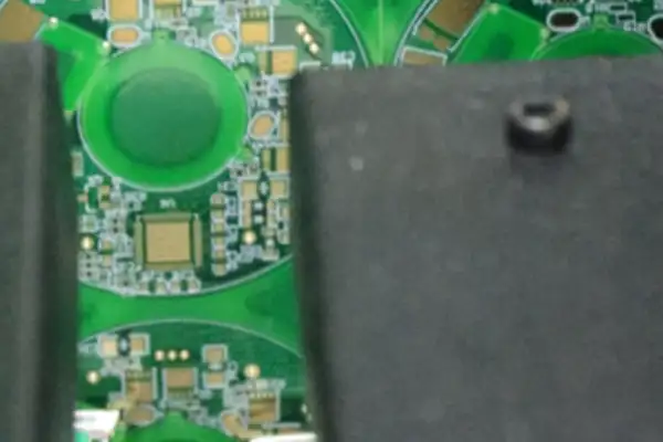
The motor drive circuit board in industrial equipment failed after long-term operation,
When selecting Printed Circuit Board Layout Services, what concerns me most are the “invisible” aspects—the things that aren’t immediately apparent. Many people get hung up on the numbers listed in technical specification tables: hard metrics such as whether a team can handle 0.4mm-pitch BGAs or if they possess experience with flexible circuitry. However, the factors that truly determine a project’s ultimate success or failure are rarely these surface-level conditions.
I once learned this lesson the hard way. I hired a team that claimed to be experts in high-density layouts. They did, in fact, complete the design files strictly according to specifications, and the deliverables appeared flawless on paper. Yet, during mass production, we discovered that a capacitor had been placed too close to a connector—so close, in fact, that the suction nozzle of the automated pick-and-place machine couldn’t physically fit in to place the component. This seemingly minor layout error necessitated manual rework on the entire batch of boards, effectively doubling our production costs.
This incident taught me that the key to evaluating a layout service provider lies in their ability to integrate engineering-centric thinking into every single detail. For instance, I once collaborated with a designer who proactively considered the width of the solder mask bridges while routing traces. Although this falls outside the traditional scope of pure electrical design, this level of insight into the manufacturing process represents the kind of truly valuable experience that sets exceptional designers apart.
Nowadays, I pay particular attention to the way designers ask questions. When they ask, “Does this interface require hot-plugging capabilities?”—rather than simply confirming pin definitions—it signals that they truly understand the operational logic of the circuit within its actual application environment. This type of application-centric thinking is far more meaningful than merely boasting about how many layers of PCBs they have designed in the past.
I’ve recently made an interesting observation: some younger engineers—despite lacking extensive experience with ultra-high-density components—actually demonstrate greater creativity when it comes to power integrity analysis. Instead of relying solely on conventional empirical formulas, they utilize simulation tools to proactively predict current paths. This capacity for dynamic adjustment and optimization is, in fact, far better suited to the rapid iteration cycles characteristic of modern product development. Ultimately, choosing a PCB layout service is much like finding a creative partner; technical specifications are merely the ticket for admission—the true value lies in those professional judgments that simply cannot be quantified.
Whenever I come across articles that make PCB design sound like some mystical art form, I can’t help but chuckle. In reality, once you’ve been in this industry long enough, you realize that “Printed Circuit Board Layout Services”—to put it bluntly—is essentially just a job of cleaning up other people’s messes.
I’ve seen far too many engineers let their imaginations run wild while drafting schematics, trying to cram every conceivable function onto a single board, only to discover—when they finally hand it over to us for layout—that there simply isn’t enough room to fit everything. At that point, we have to go back and re-evaluate the actual physical dimensions of every single component; even something as small as an 0805 resistor requires careful deliberation to determine its optimal placement.
Handling RF circuitry is perhaps the ultimate test of patience. Some people assume they can just run a trace wherever they please, but in reality, a mere 0.1-millimeter deviation in microstrip width can completely throw the impedance out of whack. I once had a client who insisted on integrating both Bluetooth and Wi-Fi onto a single board; the result was that the noise generated by the digital circuitry completely drowned out the RF signals.
When it comes to routing, one simply cannot be too rigid. While textbook principles—such as length matching—are undoubtedly important, real-world projects often require making trade-offs between performance and cost. For instance, I’ve seen plenty of instances where a design could have been perfectly realized using standard FR4 material, yet the client insisted on springing for high-end board substrates—a classic case of throwing money away unnecessarily.
The biggest headache arises when dealing with clients who possess only a superficial understanding of circuit design—the kind who point to the vias beneath a BGA package and ask, “Can’t you just pack them in a little tighter?” What they fail to realize is that if vias are spaced too densely, not only do drilling costs skyrocket, but it also becomes impossible to maintain the minimum insulation clearances required for basic electrical safety.
Flexible PCBs represent another major trouble zone. Many people assume they can be bent and twisted with total impunity; in reality, the orientation of the copper traces within the flex zone requires meticulous planning. If handled improperly, the traces can snap after being bent just a few times.
Ultimately, good PCB layout isn’t about chasing theoretical perfection; it’s about finding the optimal balance point that best meets the specific requirements at hand. It’s a lesson that one often has to learn the hard way—by stumbling and making mistakes—before it truly sinks in.
Whenever I look at complex PCB design schematics, a single question always crosses my mind: Why do so many people seem to believe that simply arranging the components in a neat, orderly fashion constitutes a finished design? In truth, the real test of an engineer’s skill often lies hidden within those seemingly haphazardly routed traces. I’ve seen countless novice designers—in their quest for aesthetic symmetry—route their traces in perfectly straight, orthogonal lines, only to end up with a chaotic mess of signal interference. I recall helping a friend revise the mainboard of an audio device last year; the original routing looked as if it had been drawn with a ruler—nothing but a succession of sharp, right-angle turns. I rerouted all the critical signal lines using smooth curves and ensured ample clearance around the power modules; the improvement in performance was immediate. Such subtle adjustments are often far more effective than simply swapping in high-end components. For instance, high-frequency signals tend to generate electromagnetic radiation and reflections at sharp corners, whereas smooth curves maintain impedance continuity—a factor absolutely critical for preserving signal integrity. Furthermore, proper power isolation helps prevent voltage spikes and noise transients from interfering with sensitive audio processing chips.
Nowadays, some companies are quick to boast about the exorbitant cost of the materials they use, yet they would be better off spending that time optimizing their grounding schemes instead. I once worked on an industrial control board project where the client initially insisted on using top-tier substrate materials; however, we later discovered that simply and completely separating the digital ground from the analog ground not only reduced costs by 30% but actually resulted in more stable performance. The application of single-point grounding techniques ensured that switching noise from the digital circuitry no longer compromised the sampling accuracy of the analog signals—a fundamental optimization that often yields far more practical value than merely piling on expensive materials.
Flexible circuit design is even more fascinating; it feels akin to tailoring a bespoke outfit for an electronic device. You must anticipate exactly how many times the board will be flexed and identify precisely which areas will be subjected to the greatest mechanical stress. On one project involving flexible circuitry for medical equipment, we implemented a mesh-like routing pattern in the high-flex zones—essentially dressing the circuit in a flexible, athletic-style fabric. By carefully calculating the bending radii and material fatigue coefficients, we employed serpentine routing on the PI substrate to effectively distribute stress, thereby extending the circuit’s operational lifespan by more than fivefold.
Recently, I’ve been experimenting with embedding sensors directly into the internal layers of a PCB, thereby eliminating the need for numerous external connectors and saving a significant amount of board real estate. Although the initial debugging process was excruciatingly tedious, the level of integration achieved in the final product was truly impressive. This approach—based on three-dimensional stacking—is bound to become increasingly prevalent in the future; after all, even modern wristwatches are now expected to pack in a staggering array of functions. By utilizing blind and buried via technology to embed temperature and humidity sensors within the second layer of the mainboard, we not only eliminated the risk of physical damage from external impacts but also achieved a truly seamless, integrated design.
Ultimately, a well-designed PCB should resemble a vascular network: wide where high current flows, narrow where precision is required, and always mindful of establishing dedicated, isolated pathways for sensitive signals. Sometimes, when I see designs where the crystal oscillator is placed right next to a switching power supply, I can’t help but break into a cold sweat for the designers; it’s no different than asking a heart patient to live right next to a rock concert venue. For instance, clock signal lines require “ground shielding” (ground guarding), and power supply lines must utilize a “star topology” to minimize voltage drop; it is precisely these minute details that determine the overall stability of the entire system.
Truly professional PCB layout services require the ability to “paint with copper”—balancing the flow of current with the specific behavioral quirks of the signals. Recently, I’ve been experimenting with using differential signal pairs for high-speed data transmission. Although they appear to be just two parallel lines, the precision required in their routing—particularly regarding isolation—is far more exacting than the soundproofing in a bachelor apartment. This involves precisely calculating line widths and spacing to achieve a 100-ohm impedance match, as well as laying down ground planes on adjacent layers to prevent crosstalk—design considerations that are absolutely critical for interfaces like USB 3.0 and HDMI.
However, what I find most striking is that even artificial intelligence has now begun to tackle PCB routing. While it may not yet be capable of solving those complex, “flash-of-inspiration” type problems, it can at least liberate designers from the drudgery of repetitive tasks. Last week, I tested a new software tool; its automated “length-matching” feature for signal traces definitely saved me a fair bit of money on coffee. Machine learning algorithms can rapidly execute T-topology routing for DDR memory; however, when it comes to RF circuits or designs with stringent EMC (electromagnetic compatibility) requirements, the experienced judgment of a human engineer remains indispensable.
Ultimately, the most captivating aspect of this industry is the constant stream of new challenges. Yesterday, we were grappling with impedance matching; today, we’re researching stretchable circuits; and tomorrow, we might be figuring out how to execute a layout on a curved substrate. With the advancement of 5G millimeter-wave technology and automotive electronics, we are even beginning to explore compensation schemes for dielectric constants that fluctuate with temperature. This continuous evolution of technical requirements ensures that every project feels fresh and exciting.
I recently had a chat with a friend who works in the smart wearables sector, and we stumbled upon an interesting phenomenon: after their team invested a significant sum to hire a professional PCB design firm to optimize their layout, the product’s return/repair rate plummeted by more than half. This incident reminded me of how people often used to assume that PCB routing was merely a matter of “connecting the dots”—as long as the circuits were electrically connected, everything was fine. In reality, anyone who has worked on complex projects understands that a truly excellent layout can be the difference between a product’s success and its failure—it can quite literally save a product.
The various PCB layout services available on the market today are, indeed, quite fascinating. I once visited their workspace and watched an engineer fine-tuning the routing of high-frequency signal lines; his intensity and focus reminded me of a surgeon performing an operation. They weren’t merely drawing lines; they were balancing seemingly contradictory requirements—electromagnetic compatibility, thermal dissipation, and mechanical durability. The layout of flexible PCBs, in particular, is far more complex than one might imagine; you have to consider minute details—such as whether the copper traces will fracture or components will detach when the board is bent—as these factors ultimately determine how many flex cycles the product can withstand.
The most remarkable case I’ve ever witnessed involved a medical monitoring patch. After a redesign of the power supply module’s routing on the PCB, the device’s standby time miraculously increased by three full days. You see, that is the true magic of layout design: without altering a single component, it can unlock the hidden potential within the hardware. Sometimes, I view this process as a form of urban planning for circuits: signal lines act as arterial roads, power lines form the transportation network, and clock circuits serve as traffic lights; a bottleneck at any single intersection can compromise the overall operational efficiency.
Many teams today are beginning to outsource their PCB design work to specialized service providers. I would argue, however, that the primary benefit isn’t cost savings, but rather the opportunity to tap into cross-industry expertise. For instance, a team with a background in designing military-grade hardware will approach reliability design for consumer electronics with far greater rigor; the value derived from this transfer of experience far outweighs the actual service fees.
Ultimately, layout design is a true test of foresight; from the moment you draw that very first line, you must anticipate whether the final assembly machine will be able to solder the components with precision—and even which specific chip is most likely to desolder if a user accidentally drops their phone. While recently helping a friend’s company evaluate several PCB design firms, I noticed a distinct pattern: truly exceptional layout engineers tend to ask particularly incisive questions—such as, “Is there a possibility this sensor might be upgraded to a multi-channel version in the future?” or “Given that this device will be used long-term in a desert environment, should we reinforce its dust-proofing?” On the surface, such questions might appear to fall outside the immediate scope of the project, but in reality, they serve to ensure the product retains ample room for future evolution.
At times, gazing upon a circuit board densely populated with components, I feel as though I am observing a form of three-dimensional art—an intricate creation that must simultaneously guarantee flawless electrical performance, facilitate efficient assembly on the production line, and remain easily accessible for maintenance and repair. A friend of mine in the industrial control sector recently vented to me, admitting that it took working through three different layout service providers before he finally grasped a fundamental truth: finding the right design team is much like finding a spouse—simply scanning a list of past projects on a price quote is useless; what truly matters is whether they are willing to invest the time to genuinely understand the underlying logic and requirements of your specific product. Ultimately, a good PCB layout is akin to crafting a resilient skeleton for an electronic product; it need not be visible to the user, yet it determines how fast the device can run and how far it can go.
I have always felt that the most fascinating aspect of PCB design is that there is never a single “correct” answer. I experienced this firsthand last year while helping a friend revise a smart home controller: despite utilizing the exact same chipset, simply shifting the position of a sensor by three millimeters completely altered the overall power supply noise characteristics.
Many people oversimplify PCB layout services, assuming it merely involves connecting components together. In reality, every routing task is like solving a three-dimensional puzzle, requiring the simultaneous consideration of seemingly unrelated factors such as electromagnetic compatibility, thermal dissipation paths, and manufacturing processes. I recall working on an industrial control board where, in order to leave sufficient clearance for future maintenance access, we managed to compress a six-layer design down to four layers—a feat that, surprisingly, resulted in even better signal integrity than the original.
Nowadays, many design teams rely too heavily on simulation software, defaulting to stacking up eight or ten layers at the slightest provocation. However, the true test of skill lies in creating a stable design within strict cost constraints. I remember a medical device project where the client initially insisted on absolute miniaturization; later, they discovered that certain test points required specific minimum spacing to meet certification standards—a requirement that, ironically, provided the layout with much-needed “breathing room.”
The challenges in automotive electronics are entirely different. During testing for one project, a prototype exhibited clock drift in an environment of minus 40 degrees Celsius; troubleshooting revealed the culprit was a decoupling capacitor positioned just half a fingernail’s width too far from the main chip. Such minute details would never surface in standard consumer electronics boards, but in the jarring, vibrating environment of a moving vehicle, they can become fatal flaws.
A truly excellent design should resemble the work of an old-world craftsman crafting traditional mortise-and-tenon joints: fitting together seamlessly while simultaneously allowing for natural expansion and contraction. I make it a habit to intentionally place a few extra “spare” vias alongside critical signal lines. While this may appear to waste space, it saves an immense amount of time and effort on “flying wires” (manual jumper connections) during the subsequent debugging phase. This kind of experiential wisdom is difficult to codify into standard operating procedures, yet it often determines whether a product remains confined to the laboratory or successfully makes its way to the market.
My recent work on several new-energy vehicle control projects has further reinforced my realization that PCB layout is no longer merely a technical exercise. For instance, the arrangement of sampling points within a Battery Management System (BMS) must not only satisfy the spacing requirements mandated by safety regulations but also facilitate ease of access for diagnostics during after-sales maintenance—a balancing act that now straddles the boundary between engineering technology and human-computer interaction. Ultimately, behind every successful circuit board lies a history of countless iterations—building, tearing down, and starting over. Those seemingly flawless design solutions actually embody the wisdom of designers who have skillfully navigated the necessary compromises with real-world constraints.
I have seen far too many people oversimplify the process of circuit board design. They assume that just finding someone capable of drafting schematics is sufficient. In reality, truly reliable Printed Circuit Board Layout Services should function more like a long-term collaborative partner. This relationship is not a mere transactional exchange; rather, it involves a deep, mutual alignment of design philosophies between both parties.
I recall a project we undertook last year. Initially, I felt that my proposed solution was already quite robust. However, our partner insisted on conducting additional testing under extreme environmental conditions. At the time, I thought they were being overly fastidious. As it turned out, the testing phase actually uncovered several potential issues. Had they not insisted on those extra rounds of testing, these problems might not have surfaced until we reached mass production.
A high-quality design service does not merely execute instructions passively; they proactively offer suggestions. For instance, regarding thermal management layout, they leveraged their past experience to adjust the placement of several components. The result was significantly superior to our original plan. Such practical, experience-driven advice is invaluable.
The testing phase often serves as the clearest indicator of a team’s professionalism. Some service providers treat testing as a mere routine formality, whereas true partners view it as a critical step in validating the underlying design concepts. They will even go so far as to formulate specialized testing protocols tailored to different product categories.
Nowadays, when selecting a collaborative partner, I place particular emphasis on their mindset—specifically, whether they truly grasp the specific problems the product is intended to solve, rather than simply mechanically translating schematics into layouts. After all, a circuit board is not a work of art; its ultimate purpose is to function reliably within a real-world operating environment.
What impressed me most was a specific team that would periodically follow up on projects that had already entered mass production to monitor the product’s performance in actual use. This attitude of sustained engagement convinced me that they genuinely cared about the success of their design work—rather than simply washing their hands of the project the moment the final deliverables were handed over.
Ultimately, seeking out PCB layout services is much like searching for a co-founder for a startup. What is required is a dual guarantee: professional competence combined with a strong sense of responsibility.
I’ve always felt that entrusting PCB layout to a professional team is a rather intriguing choice. Many people might assume, “Isn’t it just a matter of drawing lines? I can handle that myself.” However, after working on several actual projects, I’ve realized that this couldn’t be further from the truth.
I recall one instance where we were struggling with a board ourselves; we went back and forth revising the component placement alone four or five times. Those seemingly arbitrary placements actually concealed hidden complexities: high-speed signal lines needed to be kept as short as possible, analog and digital sections had to be isolated from one another, and heat-generating components required careful consideration regarding thermal dissipation paths. Later, we engaged a professional PCB layout services team to take over, and the very first thing they did was completely restructure the entire layout.
Interestingly, they didn’t rush to route the traces; instead, they took the time to understand the functional characteristics of each individual component. A senior engineer on their team once told me that a good layout is like the opening moves in a game of chess: if you get the first few steps right, everything else falls naturally into place. They even took into account details we hadn’t even noticed—for instance, how the package type of a specific capacitor would influence the nozzle selection on the pick-and-place machine, or how two seemingly unrelated components required a specific clearance between them to accommodate the manufacturing process.
What surprised me most was their approach to cost management. On one occasion, we wanted to use a cheaper connector model but were advised against it. It turned out that particular model was prone to cold solder joints during assembly, which would have effectively doubled our post-sales support costs. This holistic, end-to-end mindset—viewing design through the lens of the entire product lifecycle—completely transformed my perception of PCB design. Now, whenever I see the younger members of our team agonizing over trace routing angles on their screens, I often find myself thinking: perhaps we should have exposed them to the working logic of these professional teams much sooner. After all, some forms of experience are simply impossible to acquire merely by keeping one’s head down and grinding away at the work.
In truth, the most valuable asset you gain when hiring a professional team isn’t the technical expertise itself, but rather the pitfalls they have already encountered and overcome. During one layout project, they insisted on rotating a specific chip by 15 degrees—a decision none of us understood at the time. It wasn’t until the pilot production run that we discovered this specific angle boosted the efficiency of our Automated Optical Inspection (AOI) process by 30%. This approach—working backward from the manufacturing requirements to inform the design—represents the true, core value of outsourcing.
Whenever I come across articles that portray PCB design as some sort of mystical, arcane art, I can’t help but chuckle. They make it sound as though designing a circuit board requires mastering some exclusive, secret technique. Having worked in this industry for over a decade, I’ve come to realize that the most critical factor of all is simply building a solid foundation in the fundamentals. Those flashy, theoretical concepts often prove useless in actual practice.
Take the RF section, for instance: many people get bogged down in parameter calculations right from the start, yet what truly impacts performance is actually the most fundamental aspect—trace routing and layout. I’ve seen far too many engineers spend all their time on simulation software, only to find that the physical prototype they eventually produce behaves completely differently. The truly reliable approach is to leave ample room for tuning and adjustment starting with the very first revision; don’t expect to get it perfect on the first try. For example, you can reserve space for π-type matching networks along critical signal paths, or design alternative solder pad options for antenna matching circuits. This flexible design strategy not only saves time on repeated prototyping but also allows for rapid parameter optimization during actual testing, helping to avoid the predicament of impedance mismatch between the idealized model and the real-world circuit.
Speaking of file management, I’ve learned that lesson the hard way more than once. On one occasion, a client was in a rush to move into mass production; after I sent over the design files, the factory called to report that a component footprint didn’t match up. After scrambling for hours to figure it out, we discovered that the file versions had been mixed up—a mistake that nearly caused us to miss our delivery deadline. Now, for every project, I create a dedicated folder to categorize and organize all the schematics, BOMs (Bills of Materials), and other documents. This is especially critical when outsourcing PCB layout services; the more clearly the files are organized, the faster the external team can provide feedback. I also include a version log within the folder, documenting the specific changes made and the date of each revision. Furthermore, I require all team members to adhere to a standardized naming convention when submitting files—for instance, using the format “ProjectName_VersionNumber_Date.” This standardized management approach significantly reduces communication overhead, ensuring that even new team members can quickly grasp the project’s file structure.
I recently took on a smart home project where the client insisted on squeezing both Wi-Fi and Bluetooth modules onto a single PCB. Initially, some team members suggested separating the layouts, arguing that the RF signals would interfere with one another. However, I insisted on placing both modules within the same physical area, relying solely on grounded vias for isolation—and the subsequent testing showed that every performance metric met the required specifications. Sometimes, so-called “conventional wisdom” can actually stifle innovation. In this instance, by intelligently planning the ground plane segmentation and incorporating shielding structures, we not only reduced the overall layout area by 30% but also further lowered material costs by utilizing a shared antenna switching circuit for both modules. This integrated design philosophy is particularly crucial for space-constrained IoT devices.
Many people assume that multi-layer PCBs are inherently superior to double-sided boards, but in reality, the best choice always depends on the specific requirements of the project. An industrial controller I once worked on utilized a four-layer PCB, yet all critical signals were routed exclusively on the inner layers. The outer layers were reserved for power and ground planes; this approach not only kept costs in check but also ensured stability. When the board manufacturer reviewed our design files, they actually commended us, noting that this layout strategy made the production process much smoother for them. This layering strategy effectively shields sensitive digital signals from external electromagnetic interference, while the expansive copper planes on the outer layers provide low-impedance paths for power distribution. Operating within a high-temperature, high-humidity industrial environment, this design maintained a failure rate of less than 0.2% for three consecutive years.
What gives me the biggest headache is dealing with clients who insist on micromanaging every detail. On one occasion, a client’s boss—claiming he had watched a few online tutorials—insisted on personally dictating the placement of every capacitor. I simply handed him a scrapped prototype board—riddled with the dense, telltale traces of extensive rework—and told him that professional tasks are best left to professionals. Ironically, that very client eventually became a long-term business partner. That incident taught me that demonstrating professional judgment through visual aids is often far more effective than mere lecturing. Nowadays, whenever I encounter similar situations, I proactively prepare impedance simulation reports or thermal analysis data, using objective metrics to establish a foundation of mutual trust.
There is a rather unhealthy trend in the industry right now where people constantly boast about the sophisticated software tools they use. In reality, no matter how powerful the tool, its effectiveness ultimately depends on the person wielding it. The most outstanding designer on my team is a career-changer—someone who started out in mechanical drafting—yet he possesses an exceptional spatial intuition; the boards he designs consistently require two fewer layers than those designed by others. This goes to show that the most valuable asset in this field isn’t technical proficiency, but rather one’s mindset. He excels at applying the principles of mechanical assembly tolerance to PCB design—for instance, using 3D component models to preemptively identify potential conflicts with heat sinks, or optimizing connector placement based on the physical structure of the enclosure. This cross-disciplinary perspective often allows him to identify systemic issues that pure electronics engineers might otherwise overlook.
I’ve always found the process of outsourcing PCB design to be quite an interesting subject. Many people assume that all you have to do is toss over a schematic and the job is done—but in reality, it’s nothing like that.
On one occasion, we engaged a PCB layout service provider. Due to a lack of upfront communication, they followed standard conventions and placed the power module in a corner of the board. It wasn’t until we reached the actual debugging phase that we discovered the power supply path was excessively long, resulting in severe voltage drop. We were forced to completely rework the layout, which ended up delaying the project by two weeks.
Consequently, I now place an extremely high priority on the communication phase that takes place before any actual design work begins. Even if it takes an extra half-day to clearly annotate the thermal requirements for every component and map out the routing paths for high-speed signals, it can save a significant amount of rework time down the road.
During the routing phase, nothing is more frustrating than encountering a team that works in isolation. I once collaborated with a company that prioritized aesthetic appeal in their routing—arranging every trace with meticulous neatness—yet completely overlooked the impedance continuity required for high-frequency signals. Ultimately, they had to add compensation circuits to salvage the design.
A truly professional team will proactively initiate reviews at critical milestones—for instance, inviting us to verify component spacing once the preliminary layout is complete, or sharing screenshots to demonstrate routing paths after the high-speed signal traces have been laid out. This transparent, collaborative approach actually proves to be far more efficient.
On one occasion, I insisted on conducting an interim review immediately after the power module routing was finished. Sure enough, we discovered that the placement of the decoupling capacitors was suboptimal; by making timely adjustments, we successfully averted potential electromagnetic interference issues. This phased inspection process is far more reliable than relying solely on a single, final acceptance review at the very end.
Nowadays, I simply skip over any service providers that boast about offering “fully automated routing.” No matter how intelligent a machine becomes, it can never replicate the intellectual synergy that occurs between human engineers; truly exceptional designs are invariably forged through a process of iterative dialogue and refinement.
In a recent project, the outsourced team proposed rotating a specific chip by 90 degrees during a design review. This seemingly minor adjustment resulted in a 30% reduction in the length of the associated signal traces. Sometimes, an outsider’s fresh perspective can reveal critical details that we, being too close to the project, might have otherwise overlooked.
I believe that when seeking PCB design services, one shouldn’t focus solely on the price list. Far more important is assessing whether the provider is willing to invest the time required to truly understand the unique characteristics of your product. The most successful collaborations are those in which both parties contribute constructive feedback and insights from their respective professional standpoints.
I’ve long felt that many people harbor a misconception regarding PCB design: they assume that once the schematic diagram is complete, the job is essentially done. In reality, however, the truly fascinating part—and the true test of one’s craftsmanship—has only just begun; it is the intricate process of translating those circuit lines into a tangible physical board that truly separates the experts from the novices.
I recall helping a friend revise a smart home controller design last year. His original schematic appeared quite orderly and well-organized, yet the actual physical boards produced from it were plagued by persistent signal interference issues. It wasn’t until I completely reworked the physical layout that I pinpointed the root cause: the power supply traces and data lines were routed far too close to one another. A few minor tweaks to the routing paths were all it took to resolve the problem. Such minute details often prove to be the deciding factor between a product’s success and its failure.
Today’s market offers a plethora of PCB layout services, yet the quality among them varies wildly. Some teams may prioritize rapid delivery above all else, inadvertently neglecting the long-term maintainability of the design. What I personally value most is a designer’s ability to approach the project from a manufacturing-centric perspective—taking into account practical factors such as the ease of component sourcing and the feasibility of future repairs. When it comes to PCB layout, my primary concern is grounding. I’ve seen far too many cases of electromagnetic interference (EMI) caused by improper grounding. I once tested an industrial control device where every parameter met the required standards, yet anomalies would consistently appear at specific frequencies. We eventually discovered the issue lay in the ground loop design; only after rerouting the ground traces did the system finally stabilize.
When selecting an outsourcing service provider, I typically start by examining how they handle high-density routing. It’s much like solving a jigsaw puzzle: you must ensure that every connection is established while simultaneously preventing mutual interference. A skilled designer can offer unexpected solutions—such as employing multi-layer routing or strategically placing vias—to optimize space utilization.
During the transition from schematic to physical product, thermal management is the element most frequently overlooked. This is particularly critical in areas densely populated with power components; if heat dissipation is not thoroughly considered, even the most brilliant design will be compromised. I make it a habit to simulate thermal paths during the layout phase—a far more effective approach than simply tacking on heat sinks after the fact.
In truth, the most enjoyable aspect of PCB design is the deep sense of satisfaction derived from creating a tangible object. Watching the intricate circuitry on a computer screen transform into a physical circuit board held in one’s hands—that transition from the virtual to the real—is truly fascinating. Of course, it’s even more perfect when the board works flawlessly on the very first attempt.
I’ve long felt that many people today harbor misconceptions regarding the discipline of PCB design. Many assume that simply hiring an engineer who knows how to draft schematics is sufficient to handle the entire process—a notion that is far too naive.
I recall an interesting phenomenon our team encountered last year while working on a smart home project. The project’s core board was required to simultaneously process Wi-Fi signals and drive motor control circuits. At the time, a junior engineer—new to the field—routed the RF module’s traces directly adjacent to the power management chip. The result? When we conducted our tests, we discovered that the device’s wireless communication range had been cut in half.
This incident drove home a critical realization: modern electronic products are becoming increasingly complex. They are no longer mere assemblages of disparate functions, but rather sophisticated fusions of diverse technologies.
Take the smartphones we use every day, for instance: they house high-speed processors, sensitive RF receivers, and high-power amplifiers—circuits of vastly different natures—all crammed into a space no larger than the palm of your hand. For these disparate elements to coexist harmoniously within such a confined space, an exceptionally meticulous and sophisticated layout strategy is absolutely essential. I have encountered numerous companies that, in an effort to cut costs, opt to have their hardware engineers double as PCB designers. The result is often a cycle of repeated revisions that ultimately delays the entire project timeline. In reality, professional Printed Circuit Board Layout Services offer far more than just drafting—more importantly, they provide a systematic design mindset.
A skilled PCB engineer should be akin to an urban planner: they must not only map out the routing of every signal trace but also anticipate the potential interactions between different circuits. For instance, will switching noise from digital circuits interfere with analog sampling? Is the return path for high-frequency signals complete? Is the segmentation of the power planes logical? These are all critical factors that require comprehensive consideration.
At times, I like to liken PCB layout to musical composition—each component acts like a musical note; while seemingly independent, when combined, they produce a completely different effect. An excellent layout allows a circuit to perform at its absolute best, whereas a poor design—no matter how high-quality the individual components may be—will fail to achieve the desired results.
Consequently, I now lean toward the philosophy of entrusting specialized tasks to specialists. Rather than having the hardware engineers on the team spend vast amounts of time mastering routing techniques, it is far more productive to let them focus on what they do best: circuit innovation. After all, everyone’s energy is finite; identifying the most suitable division of labor is the key to maximizing the entire team’s efficiency.
The motor drive circuit board in industrial equipment failed after long-term operation,
Many 5G antenna PCB designs rely too much on simulation, but ignore
While collaborating with a smart wearables team to select a semiconductor flex
• Expert in Small-to-Medium Batch Production
• High-Precision PCB Fabrication & Automated Assembly
• Reliable Partner for OEM/ODM Electronic Projects
Business Hours: (Mon-Sat) From 9:00 To 18:30