
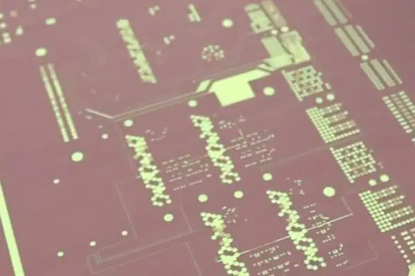
Industrial Automation PCB Reliability: How to Achieve 10+ Years of Stable Operation
In the field of industrial automation, people often pay attention to AI
I’ve seen too many people underestimate the complexity of multilayer PCB manufacturing. They think they can just find any manufacturer to handle complex design requirements. In reality, after working in this industry for over ten years, I’ve noticed a pattern: manufacturers who truly excel at making multilayer boards possess a special quality – they have both a craftsman’s spirit and the ability to keep up with technological advancements.
I remember last year a client came to me complaining about problems with their previous supplier’s eight-layer board design. Looking at the design, I immediately understood the problem. Many engineers now pursue higher layer counts but neglect the compatibility of the basic manufacturing processes. Sometimes a six-layer board is more stable than a ten-layer board; the key is how you plan the signal and power layers.
The electronics industry has indeed experienced explosive growth in the last five years, but this doesn’t mean all products need to pursue the highest layer count. In a medical device project I worked on, the initial design used a twelve-layer board, but we later found that an eight-layer board could fully meet the requirements through layout optimization, saving 30% in costs. The essence of multilayer PCB manufacturing is not about stacking many layers, but about ensuring perfect synergy between each layer.
There’s an interesting phenomenon: newcomers tend to be obsessed with technical parameters, while experienced professionals focus more on the manufacturer’s production details. For example, some manufacturers can control impedance errors within 5%, while others can’t even guarantee 10%. This difference might not be significant in ordinary double-sided boards, but it’s a world of difference in high-frequency multilayer boards.
What the PCB industry lacks most is not advanced equipment, but talent that understands how to balance design and manufacturing processes. During a visit to a large manufacturer’s multilayer PCB fabrication workshop, I noticed their engineers were using magnifying glasses to inspect each via fill. This seemingly simple step is actually crucial in determining product lifespan.
In fact, there’s a very intuitive way to judge a manufacturer’s capabilities: observe their attitude towards simple orders. Manufacturers who take the production of four-layer boards seriously are often more reliable when it comes to sixteen-layer boards. After all, process discipline is ingrained in their culture and doesn’t change with product complexity.
Many startup teams blindly pursue “flagship configurations,” unnecessarily complicating simple problems. I often advise them to first clarify their core needs before deciding on the number of layers. A good design utilizes each circuit layer effectively, rather than simply stacking layers for the sake of showing off.
Explosive growth brings not only opportunities but also a restless mindset.
Having worked with multilayer PCBs for many years, I’ve gradually discovered a common misconception about material selection – the belief that expensive materials are always better. Material selection is like choosing clothes; it depends on the occasion. Standard FR materials are perfectly sufficient for most consumer electronics products; there’s no need to insist on high-speed materials. I’ve seen many projects where, in pursuit of impressive parameters, high-end substrates were used, resulting in doubled costs.
Once, I helped a client revise a design. They initially specified a certain brand of low-loss material for their mobile phone motherboard. After reviewing the signal frequency, I found it didn’t require that level of material and suggested switching to a mid-range FR material. The money saved could then be used to improve heat dissipation, resulting in a more balanced overall performance. The biggest mistake in multilayer PCB manufacturing is over-engineering without considering actual needs.
The choice of copper foil is particularly interesting. Conventional designs can handle most situations with 1-ounce copper thickness, but some people worry about insufficient current and insist on thicker copper. In reality, increasing copper thickness affects etching precision and can be a burden on fine lines. I usually calculate the actual current requirements first before deciding whether to increase the copper thickness; sometimes optimizing the trace width is more effective than simply increasing the copper thickness.
I remember a power module project where the client insisted on using 2-ounce copper foil for high current. Later simulations showed that the key wasn’t the copper thickness but the heat dissipation design. We added several thermal vias in the heat-generating area, and the problem was solved with standard copper thickness. Multilayer board design really can’t be based on single factors alone.
Material matching is where the real skill lies. Different combinations of prepreg materials affect dielectric thickness; sometimes a slight adjustment to the stacking structure can improve impedance control. Once, while working on an RF board, we tried three different glass fabric specifications before finding the most suitable thickness. This kind of fine-tuning can’t be seen in simulations; it relies on practical experience.
Now, I feel sorry for those who blindly pursue high-end materials. Good multilayer board manufacturing should prioritize the most economical choice while meeting performance requirements, because the product ultimately needs to face the market.
Every time I see those complex circuit board designs, I wonder how many processes were involved. Especially the electroplating process in multilayer PCB manufacturing – that seemingly simple step actually hides many intricacies.
I remember once our factory received an order for a high-density board. Those boards required a large number of micro-vias. Initially, when we followed the conventional electroplating process, we found that the conductivity resistance of some vias was abnormally high. Upon analysis, we discovered that the plating was too thin in the middle of some deep holes. This situation is quite common, especially when dealing with boards with a high aspect ratio.
Later, we adjusted the parameters of the pulse electroplating, segmenting the current density and time. Specifically, in the initial stage, we used a lower current to allow the hole walls to form uniform crystal nuclei, and then gradually increased the current for filling. This adjustment increased the thickness of the copper layer in the middle of the deep holes by nearly 30%, with immediate results.
In fact, the most challenging aspect of multilayer PCB manufacturing is not how advanced the equipment is, but the ability to control every detail. Take the post-drilling treatment, for example; many people think that simply drilling the holes is enough, but what truly affects subsequent processes is the quality of the hole walls. If the residual resin after drilling is not cleaned properly, subsequent chemical copper plating will have problems, leading to insufficient local adhesion.
I’ve seen some factories shorten the desmearing time to meet deadlines, resulting in boards that passed initial testing but started experiencing intermittent failures after six months of use. This kind of problem is often only discovered when the product experiences mass failures in the market, but the damage has already been done.
The graphic transfer stage is also a place where mistakes are easily made. Once, when we were making boards with high impedance control requirements, misalignment during exposure caused jagged edges on the traces, and we had to scrap the entire batch and redo them. Now, we require an optical inspection after development, which adds a little time but avoids greater losses.
After working in this industry for a long time, you’ll find that every step is interconnected. A small oversight in an earlier process can be magnified into a fatal defect in later stages. Sometimes customers ask why boards of the same specifications have such different prices; the difference lies in the handling of these details.
The industry is now pursuing finer line widths and smaller hole diameters, which places higher demands on manufacturing processes. But no matter how the technology changes, the core remains the precise control of each step. After all, even the most advanced equipment needs human operation, and experience is often the most valuable asset.
Recently, we’ve been experimenting with a new electroplating additive, and the results are quite good, especially in improving the uniformity of deposition at the bottom of deep holes. However, new things always require repeated verification before large-scale application; this is a characteristic of manufacturing – stability first, speed second.
Ultimately, making circuit boards is like cooking; the heat and seasonings must be just right. Every master craftsman has their own unique insights, and these insights are often summarized from countless failures.
I’ve always felt that when discussing multilayer PCB manufacturing, many people easily get lost in the maze of technical details, neglecting its most essential aspect – it’s actually an art of balance. I remember when I first started in this field, I always thought that the more layers, the better, and the higher the precision, the more impressive. But later I realized that wasn’t the case at all.
Once, we designed a six-layer board application, but the customer insisted on an eight-layer structure. The cost doubled, and it also brought about heat dissipation problems. In fact, for most consumer electronics products, a four-to-six-layer design is often the most economical and practical choice.
What fascinates me most about multilayer PCB manufacturing is its flexibility. The same functional requirements can have completely different implementation paths. For example, the smart home controller we recently made uses an asymmetrical stacking design, cleverly separating the power and signal layers.
When it comes to the word “precision,” many people’s first reaction is how small the line width and spacing should be. But I think true precision is reflected in the understanding of material properties. How much deformation will the difference in the thermal expansion coefficients of different dielectric layers cause at high temperatures? This is the key to determining the yield rate.
I’ve seen too many engineers focus all their energy on circuit design, yet have only a superficial understanding of the PCB manufacturing process. In fact, understanding the boundary conditions of the manufacturing process is more important than pursuing extreme parameters.
Now, when many people discuss high-layer count boards, they always talk about mobile phone motherboards. But I think applications in the industrial control field better demonstrate the value of multilayer PCBs. Maintaining stable operation for over ten years in harsh environments is far more convincing than the impressive data measured in a laboratory.
Recently, a project particularly resonated with me – we designed a PCB board for medical equipment, considering both electromagnetic compatibility and mechanical strength. Ultimately, we achieved the desired results through a special layering scheme.
Ultimately, good PCB design isn’t about piling on technology, but about precisely matching the requirements.
Sometimes I feel it’s a pity to see colleagues blindly increasing the number of layers in pursuit of new technologies.
Truly excellent engineers should understand how to find the optimal balance between cost, performance, and reliability.
I’ve been pondering something lately – why are some circuit boards exceptionally stable, while others are prone to problems? This reminded me of a project I participated in last year, where we encountered a particularly tricky situation.
It was an eight-layer board used in medical equipment. Initially, the sample tests went well. However, during environmental aging tests, the third batch of products suddenly showed signal instability. We investigated for a long time and finally discovered that there was a deviation in the impedance control of one of the layers.
This made me realize that multi-layer PCB manufacturing is not simply a matter of pressing several layers together. The complexity doubles with each added layer. For example, tiny fluctuations in temperature and pressure during the lamination process can lead to micron-level misalignment between layers. This deviation can cause serious signal integrity problems during high-speed signal transmission. Especially when the dielectric thickness between the signal layer and the reference plane is uneven, the characteristic impedance will deviate from the design value.
In fact, many manufacturers are now starting to pay attention to early design simulation. I know an engineer who is particularly good at this; he always says that good design can avoid 80% of later problems. That’s absolutely true. He frequently uses 3D electromagnetic field simulation software to predict power integrity issues, and by optimizing the layout of decoupling capacitors in advance, he can keep power supply noise within 50mV.
Speaking of reliability testing, I think temperature cycling is the most challenging part. Last year, we had an automotive electronics project that required stable operation between -40 degrees Celsius and 125 degrees Celsius. We found that the difference in thermal expansion coefficients of different materials caused mechanical stress on the solder joints during extreme temperature cycles. After 1000 cycles, some BGA package ball grid arrays developed microcracks.
Sometimes I think that designing circuit boards now is completely different from ten years ago. Previously, the focus was on whether the circuit worked at all; now, we have to consider whether it works reliably under various extreme conditions. For example, high-speed interface design now requires considering phenomena like intersymbol interference and ground bounce, which need to be verified using a network analyzer with time-domain reflectometry capabilities.
Recently, I encountered a customer in industrial control who is particularly concerned about long-term stability because their equipment may need to run continuously for several years without downtime. They require accelerated life testing, simulating long-term use by increasing the ambient temperature. Typically, this involves continuous operation at 85 degrees Celsius for 2000 hours without any failures.
Ultimately, multi-layer PCB manufacturing is like preparing a delicate dish; the ingredients must be good, the cooking time precise, and every step must be meticulous. From the baking temperature control during core board pre-treatment to the exposure energy calibration during pattern transfer, and the real-time monitoring of chemical concentrations in the copper plating process, every parameter needs strict control. For example, a 5% deviation in the activator concentration during copper plating will affect the density of the plating on the hole walls.
I increasingly feel that this industry needs more patient and meticulous people. Those who try to take shortcuts often end up paying a much higher price. One colleague skipped the impedance test calibration step to meet a deadline, resulting in a 15% deviation in differential impedance for the entire batch of boards, leading to mass rework on the customer’s production line and compensation exceeding three times the project profit.
Now, I see that successful manufacturers all have one thing in common: they are willing to invest in testing, both in equipment and personnel. For example, they purchase automated optical inspection systems to check for defects in fine lines, use flying probe testers for 100% continuity testing, and equip themselves with X-ray inspection equipment to detect hidden soldering problems. This might be why some manufacturers can produce high-end multilayer PCBs while others can only serve the low-end market. High-end customers typically require detailed process capability index reports, demonstrating that the CPK values of key production parameters are maintained above 1.67. This means that the process capability is sufficient to guarantee a Six Sigma quality level.
Ultimately, quality is something that cannot be faked; time will prove everything. A factory manager with twenty years of experience often says that circuit boards are like a mirror; every detail of how you treat them will ultimately be reflected in the product’s reliability. Those who cut corners on material selection may not see problems in the short term, but after one or two years of use, phenomena such as decreased insulation resistance and metal migration will appear.
I’ve always felt that the most fascinating aspect of multilayer PCB manufacturing is how it transforms a two-dimensional plane into a three-dimensional structure, like building with blocks. Many people think that circuit boards are as simple as drawing lines and etching, but those who have actually worked with multilayer boards know that the most difficult part is not drawing the design, but aligning the dozens of layers of circuitry perfectly.
I remember visiting a factory once and seeing workers aligning the processed inner core boards onto the prepreg sheets. Their concentration was like that of a surgeon performing surgery. Even a slight deviation of a few tens of micrometers would render the entire board unusable. At that time, I realized that this kind of precision work couldn’t be done solely by machines; the skilled hands of experienced technicians were crucial.
The curing process is quite interesting. Once, we tried adjusting the heating curve ourselves, but the resin flowed unevenly, and the edges of the board bulged. We later realized it’s like baking a cake; even a slight difference in temperature can drastically affect the outcome. Especially since the inner layers of the circuit are pressed together in the middle, there’s no chance to rework it, so every step in the early stages must be handled with extreme care.
Some manufacturers skip the browning process to save time, but that dark coating is actually crucial for preventing delamination. I’ve seen too many cases of inner layer separation due to insufficient bonding strength, all caused by cutting corners in the manufacturing process.
Ultimately, making multilayer PCBs is a test of overall perspective; everything from material selection to process parameters must be considered comprehensively. Sometimes the most inconspicuous steps are the ones that determine success or failure, a principle that holds true across all manufacturing industries.
I’ve seen many engineers meticulously design circuit layouts but have only a superficial understanding of the manufacturing details of multilayer PCBs. In reality, the reliability of the board is often determined by seemingly insignificant details – such as whether the solder pad treatment is done correctly. Once, our team found abnormal signal attenuation while testing a high-frequency signal board. After much troubleshooting, we discovered it was due to uneven copper plating thickness causing impedance mismatches. This kind of problem is impossible to detect on the design drawings; it only becomes apparent during actual production.
High-density designs are becoming increasingly common, but many people blindly pursue narrow line widths and spacing while neglecting more fundamental aspects. For example, the accuracy of the solder mask opening. If the solder mask bridge around the pad is too narrow or misaligned, the solder paste can easily overflow during reflow soldering, causing short circuits. I’ve seen some factories use extremely thin solder mask ink to save costs, resulting in blistering and peeling in humid and hot environments. These seemingly trivial details directly affect the lifespan of the entire board.
When it comes to surface treatment, each method has its own intricacies. Chemical immersion silver is inexpensive but prone to yellowing over time, while the ENIG process is stable but extremely sensitive to plating parameters. We once had a batch of control boards with BGA packages where a difference of a few seconds in the gold plating time led to a surge in soldering defects. Now, for precision components, I prefer the organic solderability preservative (OSP) solution; although more expensive, it offers much more reliable compatibility.
The true test of a manufacturer’s capabilities lies in their micro-hole processing capabilities. Some small factories claim to be able to do laser drilling, but their actual hole diameter tolerance can be as high as ±20%, which is completely unusable for high-density boards. Sequential lamination technology sounds impressive, but in essence, it’s all about controlling lamination precision. I once visited a Japanese-owned factory’s workshop, and their lamination machine’s temperature fluctuations were controlled within ±1.5℃ – that’s true expertise.
Recently, while working on a 16-layer communication backplane, I deeply appreciated the importance of via filling and plating. To save time, we chose a new supplier, but the vias had voids at the bottom. During thermal shock testing, they cracked, resulting in the entire batch of boards being scrapped. This taught me that you can’t cut corners on high-density boards.
The most easily overlooked aspect is electrical testing. Flying probe testing is now standard, but many manufacturers’ test coverage is simply insufficient. We learned this the hard way when all the boards passed testing, but the customer found a reset signal wasn’t connected during boundary scan testing. It turned out the test program missed this network, proving that even the most sophisticated manufacturing process requires a rigorous quality inspection plan.
I’ve recently noticed an interesting phenomenon: many people think multilayer PCB manufacturing is just a step-by-step, standardized process. But it’s not like that at all; it’s more like preparing a complex dish that requires repeated adjustments. Sometimes, even if you follow the recipe and add all the ingredients, a slight difference in cooking time can completely change the taste.
I remember a project our team took on last year where a designer was particularly fixated on theoretically perfect symmetry in the layer stacking plan. However, the samples showed slight misalignments in the inner layers, and it took three adjustments to find the problem. We later realized that instead of pursuing absolute symmetry, it’s better to allow for appropriate manufacturing tolerances. These seemingly imperfect designs actually provide breathing room for the manufacturing process. For example, in the arrangement of core boards and prepregs, appropriately increasing the balanced copper area in asymmetrical structures can effectively counteract stress deformation during lamination. This dynamic balance thinking, based on material properties, is more in line with actual production needs than simply pursuing geometric symmetry.
The most easily overlooked aspect during the design phase is the matching of material thermal expansion coefficients. Once, when working on a 16-layer board, we encountered a strange situation—all tests passed at room temperature, but open circuits appeared after high-temperature aging. We later discovered that the large difference in CTE between two dielectric layers caused stress concentration. This lesson made me realize that multilayer design shouldn’t only focus on electrical parameters but also consider the compatibility of physical characteristics, like assembling building blocks. For example, when FR-4 and Rogers 4350B are laminated together, the 3 ppm/°C difference in their Z-axis expansion coefficients can cause microcracks during thermal cycling. This requires mitigation through adjusting the glass fiber weave direction or adding buffer layers.
There’s a common misconception about hole size design – many people think smaller is better. In reality, excessively small holes not only increase drilling difficulty but also lead to uneven copper plating inside the holes. We once tested 0.15mm microvias and found that the yield rate dropped sharply when the board thickness exceeded 1.6mm. When customers request extreme aperture sizes, I always advise them to first evaluate the critical parameter of board thickness-to-aperture ratio. Especially with PTFE materials commonly used in high-frequency, high-speed boards, their soft characteristics can cause fiber tearing in the hole walls when the aspect ratio exceeds 8:1. In such cases, a combination of stepped drilling or laser drilling processes is required.
My recent experience with a medical equipment project further highlighted the importance of deep collaboration between design and manufacturing. The customer’s initial design was perfect in simulation, but during actual production, we found that the blind vias were located exactly on the panel separation line. After five rounds of video conferences and adjustments, we finally resolved this issue by optimizing the routing layout. This iterative process of collaboration is the most interesting part of multilayer PCB manufacturing. For example, changing the original mechanical panel separation to laser cutting not only avoided sensitive areas but also doubled the milling cutter lifespan by adding auxiliary holes in the process edge.
In fact, whenever I receive a new design proposal, I prefer to look at seemingly unimportant details first, such as the treatment of right angles in the silkscreen frame or the distribution pattern of test points. These often reflect the designer’s understanding of manufacturing processes. Sometimes, a simple teardrop pad adjustment can improve the yield rate by several percentage points. This kind of tacit understanding hidden in the details is key to efficient collaboration. For example, using a 45° staggered arrangement for test points in the BGA area, instead of a straight line layout, prevents probe slippage and provides space for rework. When faced with complex design requirements, we now advise clients to conduct 3-6 layers of prototype verification. This is not only to test electrical performance but also to confirm the manufacturer’s actual process capabilities. On one occasion, a client insisted on skipping prototyping and going directly to mass production of a 22-layer board. The result was that the entire batch of boards had to be scrapped due to the need for adjustments to the lamination parameters. This avoidable loss was quite unfortunate. During the prototyping phase, embedded thermocouples can be used to monitor the lamination temperature curve, which is particularly important for controlling resin flow in HDI boards.
Truly excellent manufacturing should be like providing designers with a technically savvy partner who understands which unconventional ideas are feasible and can anticipate which details might need adjustment. There are no standard answers in this process; each collaboration is a new exploration. For example, we recently assisted a client in changing the copper pillar interconnects on a ceramic substrate to a copper ink filling structure. This not only solved the thermal matching problem but also improved thermal conductivity by 30%. This kind of innovation often arises from a deep understanding of the material limitations at the manufacturing end.
In the field of industrial automation, people often pay attention to AI
Ever wonder how your phone maintains a stable signal? It relies on
When selecting components for a security monitoring system, most attention goes to
• Expert in Small-to-Medium Batch Production
• High-Precision PCB Fabrication & Automated Assembly
• Reliable Partner for OEM/ODM Electronic Projects
Business Hours: (Mon-Sat) From 9:00 To 18:30