
Why the Circuit Board Beneath the Camera Determines Whether Your Surveillance System Holds Up for Years
When selecting components for a security monitoring system, most attention goes to
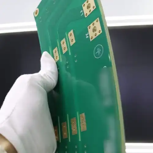
I’ve always found RF PCB design particularly interesting—it’s not like ordinary circuit boards where you just lay out the traces and you’re done. I remember once working on a hybrid PCB project using a PTFE substrate, only to find that the material was so soft, like modeling clay; even a slightly faster cutting speed resulted in edges that looked like they’d been chewed by a dog.
Later, I realized the problem was with the material properties—PTFE causes significantly more wear on drill bits than ordinary FR4. Sometimes, after processing twenty boards, we had to replace the drill bits, otherwise the hole accuracy would drift outside the tolerance range.
The most troublesome part was the cavity structure inside the multilayer board. That time, we tried using three lamination steps to make an RF board with a shielded cavity, but after the second step, we found that the prepreg had squeezed out from between the layers, like jam leaking from a sandwich cookie.
Laser cutting could have solved this problem, but the boss thought the equipment was too expensive, so we had to bite the bullet and use a milling cutter for controlled-depth grooving—during that time, I spent every day staring at the microscope, checking the distance between the groove bottom and the lower copper foil, afraid that one day I would cut too deep and pierce the signal layer.
The electroplating process was also vastly different. Before copper plating PTFE boards, the hole walls had to be treated with plasma, otherwise the metal layer wouldn’t adhere. Ordinary FR4 boards, on the other hand, could be processed simply by soaking them in a chemical solution. Every time I see young engineers diving straight into drawing schematics for RF design, I want to remind them: spending half a day researching material properties is far more cost-effective than three weeks of rework later. After all, there’s a whole universe of manufacturing processes between the schematic and the finished PCB.
When dealing with mixed PCBs, I’ve noticed that many people overlook a crucial detail: the differences in how different materials react to the manufacturing process are much greater than we imagine. For example, some processes work well with PTFE but fail with FR4; the resulting surface roughness can lead to problems with subsequent copper plating. This isn’t a problem with the material itself, but rather a lack of proper process adaptation.
RF circuits have particularly stringent requirements for vias. I’ve seen many cases where insufficient via filling led to uneven heat dissipation and a significant drop in high-frequency signal quality. Filling with conductive material sounds simple, but it requires a lot of accumulated experience. Density differences and flow control all affect the final result. Once, we had a board where uneven distribution of the filling material caused localized overheating, almost leading to a complete project rework.
Drilling accuracy is just the basics; the real test of skill lies in the subsequent processing steps. Inadequate cleaning or poor control of plating thickness will render even the best filling materials ineffective. RF performance is extremely sensitive to tolerances; sometimes, micron-level deviations are enough to cause specifications to be exceeded. Looking back at those failed cases, it’s clear that the initial details weren’t handled properly.
I think the biggest mistake in making these kinds of boards is applying fixed process parameters. Every time a new material is introduced, you have to rediscover the optimal process. Experience can’t be rushed, but by taking the time to record the effects of each adjustment, you can gradually develop your own judgment and logic. Recently, we improved the yield of several high-frequency boards by optimizing the filling process.
I’ve seen many people working on high-frequency circuits who are overly reliant on material parameters, thinking that choosing a low-loss substrate will solve all problems. In reality, the factors that truly determine RF performance are often those seemingly insignificant details—for example, whether the FR-4 prepreg you’re using will produce bubbles during lamination. Once, a project used three different dielectric constant materials in a mixed PCB lamination, resulting in phase inconsistency that made calibration impossible.
Anyone working with RF circuits has probably experienced this despair: the simulation curves look perfect, like something out of a textbook, but the actual measurements look like an electrocardiogram. The problem often lies in the mismatch of thermal expansion coefficients of the materials. Especially when high-frequency laminates and ordinary FR materials are combined, if the lamination temperature curve is not properly adjusted, the board will warp like a potato chip after cooling.
A common misconception is that mixed structures require special adhesives. In fact, adjusting the copper foil thickness is often more effective—using thin copper in the RF trace area to reduce edge effects and thick copper in the power supply section to lower impedance is a more practical approach than simply piling up expensive materials.
I remember one time we made an antenna feed line on the middle layer of a mixed PCB, with ordinary FR material used for shielding on both sides. We found that a dielectric thickness deviation exceeding 5% would worsen the standing wave ratio to an unacceptable level. Later, we discovered that the unevenness of the press platen caused uneven local pressure, a problem that couldn’t be detected by simply looking at the material datasheet.
Now, when I see manufacturers advertising “full range of high-frequency laminates,” I always ask them whether their laminating machines have real-time pressure monitoring. After all, RF performance isn’t just about buying the most expensive materials; it depends on whether the entire manufacturing chain can maintain that 0.1 mm thickness tolerance.
Sometimes the simplest solution is the most effective, such as filling the cavity areas with low-loss silicone gel, which can both control impedance and relieve mechanical stress. Instead of pursuing new materials, it’s better to thoroughly understand existing processes—after all, even the best mixed PCB design is only useful if it can be mass-produced.
I’ve been thinking a lot about mixed PCBs lately, especially those used in RF applications. Many people think that simply stacking different materials together will solve the problem, but it’s not that simple.
I remember an interesting phenomenon I encountered last year while debugging an antenna module for a friend. We were using a combination of a special high-frequency material and conventional FR4. Theoretically, this should have improved signal quality, but unexpected interference occurred during testing. Later, we discovered that the difference in expansion coefficients between the two materials caused minute deformations that affected the RF performance.
When choosing materials, you can’t just look at the numbers on the datasheet; the actual performance in real-world applications is more important. Some combinations look perfect in the lab, but various strange problems can arise in real environments. For example, inconsistent shrinkage rates of different layers during temperature changes can create internal stress in the entire board, and over time, delamination may even occur. I prefer to learn from practical case studies. Once, we tried a hybrid design using a new ceramic substrate and traditional PCB materials. Initially, we were worried about high-frequency losses, but we found that with proper layout of the RF circuitry, we could achieve more stable signal transmission. The key is to find the right placement for materials with different characteristics, rather than simply stacking them together.
Many engineers now rely too heavily on simulation software data. In reality, building and testing several prototypes often reveals more detailed problems. For example, improper temperature control during soldering can cause micro-cracks at the junctions of different materials. These subtle defects are invisible on the drawings but can significantly affect product lifespan.
The biggest pitfall in hybrid PCB design is making assumptions. I think it’s better to thoroughly understand the characteristics of basic materials than to pursue the latest and most expensive ones. Sometimes, a simple combination of materials, if designed properly, is more reliable than a complex solution, especially in RF applications where stability is often more important than peak performance.
When selecting components for a security monitoring system, most attention goes to
Behind the mobile signals we rely on daily lies the sophisticated engineering
Many assume that wireless communication PCBs require expensive high-frequency materials. This guide
• Expert in Small-to-Medium Batch Production
• High-Precision PCB Fabrication & Automated Assembly
• Reliable Partner for OEM/ODM Electronic Projects
Business Hours: (Mon-Sat) From 9:00 To 18:30