

Automotive Rain Sensor PCB: How Optical Paths, Potting, and Fabrication Quality Decide Field Performance
Do you think a rain sensor is just a simple circuit board?
I used to think that drawing a board that could run was enough, and that a VoIP gateway was just a chip packaging analog voice and sending it to the network port, so how complicated could it be. Then, the moment our second-revision prototype powered up and the ringing current started, the microphone channel was simply stunned. That crackling noise infected the whole signal chain along the feed loop, while the digital part kept running as clean as ever, and the sound on the analog end was like being stuffed into a washing machine drum.
Where was the problem? We invited an old fellow who had spent over a dozen years in a telecom board factory over for tea, and he turned the board over and over for two minutes and then tossed out a sentence
Later we redrew the requirements and specifically went looking for multilayer board suppliers who can do mixed high-speed digital and high-voltage analog, not the universal kind of factory that says at the drop of a hat that it can make any number of layers. You ask them: is the dielectric loss tangent of your FR-4 board material stable at the ringing frequency? Can the inner layer copper thickness withstand the heating of continuous feed current? When mixed lamination is spliced, how do you guarantee the reliability of HDI microvias in the high-voltage area? Those who cannot answer can basically be passed. I met two quite interesting ones. One was an HDI board factory specializing in high-density interconnect, who directly suggested putting the feed traces of the four FXS channels on an independent inner power layer, using wide copper plus thermal islands to share the heat, and changing to a higher-Tg substrate between the power layer and ground layer, just so that after being inserted in a rack and running for a long time, hot spots would not produce interlayer micro shorts. The other was a factory making high-speed backplanes, who cared more about our network port and DDR traces, readjusted the differential impedance for us, re-fanned out the address lines that we had mistakenly believed were done once length matching was finished, and added via arrangements for dynamic reference layer switching.
A trader who sells multilayer boards will simply not talk to you about these things, since they care only about how many square meters you order. A real multilayer PCB manufacturer, especially one that manages its own electroless copper line and laser drilling equipment, fears even more than you that a board will blow up in a customer’s rack, because once there are burned holes or high-voltage creepage, the whole batch has to be reworked. The HDI supplier we later stabilized on sent a stackup confirmation sheet before every prototype, marking the dielectric thickness, residual copper rate and withstand voltage of every layer clearly, and even asked in advance whether the silkscreen ink could withstand the high-humidity environment test after wave soldering. With more details like this, you dare to hand over the mainboard of a four-port, eight-port or even thirty-two-port gateway to them for material release.
Put plainly, the VoIP gateway board is not testing how slick your drawing software skills are but testing whether you have in hand the supply chain that can handle three things kneaded together: high-voltage isolation, multilayer mixed lamination and high-speed signal integrity. When looking for multilayer board prototyping, do not look only at how many layers and how much per square meter, but ask them whether they have previously made telecom backplanes with -48V live insertion protection, and whether they have handled cases where cold soldering of the thermal pad under the SLIC chip burned the feed. An HDI PCB manufacturer that can get real application feedback is often far more reliable than a supplier that only says no problem, because in the end you do not want a beautiful cross-section report but hardware that runs telephone service quietly in the cabinet, can withstand a twenty-four-hour full-load ringing test, and whose microphone end remains so clean that only the human voice is left.
After several years tinkering with VoIP gateways, the one sentence I most want to tell newcomers to hardware is this: do not be led by the nose by that SLIC theory, wanting at every turn a twenty-layer board and feeling at ease only after finding an HDI PCB manufacturer. I have seen too many people start by looking up papers on tracking battery power and mixed-signal isolation, and then spend two months drawing the layout airtight, and when the board comes back and is measured, the off-hook noise is larger than with an ordinary four-layer board. The problem is not complicated. We simply over-design the analog front end that should not be too precise in the first place.
For a while I was also trapped in this loop. It was an eight-port FXS gateway, with a Qualcomm solution with DSP as the main controller, and that thing itself ran very hot. At first I took the easy way and directly used a multilayer board manufacturer I had long worked with, six layers with conventional FR408HR. The result was that after an hour at full load, near the SLIC chip it was too hot for a hand to touch, and crosstalk between channels began to show. My first reaction at the time was that the stackup was not right and I had to switch to HDI, so I found another HDI PCB supplier and had them produce a 2+N+2 stackup scheme, and also re-partitioned the input and output ports. Money was not spared, and when the batch came back, heat dissipation was only slightly better, but the crackling noise during ringing was more obvious, and the DDR3 on the high-speed port side occasionally ran away. Only on disassembly and debugging did I find that the parasitic inductance of the laser holes on the HDI board was much larger than estimated, and the decoupling loop of my 48V feed happened to pass through these vias, with switching noise all coupled into the analog ground. This is the consequence of blindly chasing process.
After going around such a big circle, what finally pinned the problem down for good turned out to be a high-speed PCB manufacturer that did not sound so high-end. What they understood was not how many orders of buried and blind vias, but they were very clear how much loss difference copper foil roughness of their own substrate can bring at several hundred megahertz, and knew which prepreg’s glue flow during mixed lamination would make the impedance of the critical signal layer float to the sky. Holding their stackup suggestion, I separately pulled two layers for the tracking power of that SLIC path, bridged the digital ground and analog ground at a single point with one component, made the DDR length-matched traces honestly follow the reference plane, and even carefully scraped the ground copper under the Ethernet PHY. A four-layer board still made the voice quality of eight interfaces clean, and the surge test also passed the first time. The heat dissipation problem was solved by adjusting board thickness and copper thickness, with no change to the number of stackup layers at all.
So now when newcomers ask me what board factory to choose for VoIP Gateway PCB design, I say it very plainly: first work out whether those low-frequency, high-voltage pits you have already stepped in are truly worth filling with a more expensive process. Much of the so-called interface noise and gateway echo is in essence power distribution and ground bounce, not a lack of a few layers of laser blind vias. Finding a multilayer board supplier who truly understands impedance control is ten times more useful than finding an HDI PCB manufacturer who only knows how to stack layers. Especially since SLIC chips today are highly integrated, paired with a decent tracking power supply design, there is simply no need to make the layout like an RF board. With the money saved, you might as well swap in a more usable high-temperature electrolytic capacitor or add a fan to the chassis, which is more practical than anything.
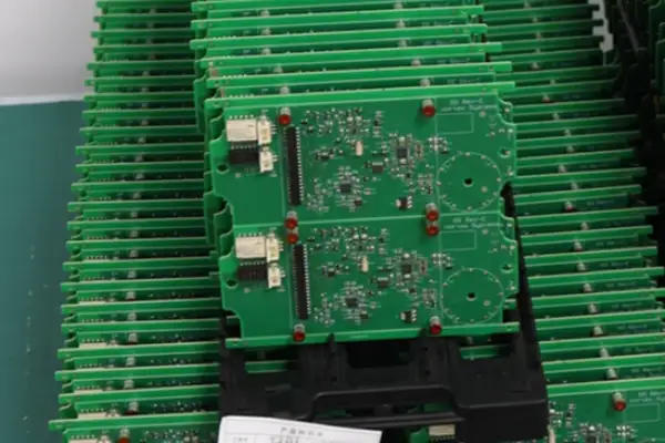
Some time ago I helped a friend look at a VoIP Gateway PCB case, with the board size stuck very tight and two dual-channel SLICs on it, and the tracking battery voltage in the power section always had glitches, directly interfering with the voice channel during ringing and sounding like old radio stations crossing. On opening and looking at the layout you know where the problem lies: the high-voltage area was squeezed together with digital signals and the plane layers were split into pieces, which plainly means the board factory did not take the minus 150V matter seriously at all. For boards from an ordinary multilayer board factory, if the inner layer withstand voltage is not enough, they cut copper to patch it for you, and after cutting, the loop inductance is large and the tracking voltage is even less stable. Later I had them switch to a proper hdi pcb manufacturer, who used laser blind vias to pull the boost part directly onto a separate power layer and re-widened the spacing between adjacent traces by safety regulations, and when the prototypes came back and were measured, the tracking response of the SLIC was as smooth as a knife cutting butter. In fact many people choosing chips stare at power consumption on the datasheet and forget that the physical implementation of the PCB is the bottom line. A dual-channel scheme seems to save area, but if the voltage drop on traces is not handled well, the chip’s internal compensation simply cannot pull it back. There are in fact not many multilayer pcb suppliers who can do this work cleanly now, and many claiming to be high speed PCB manufacturers show timidity once they meet analog high-voltage mixed design. My own habit is that whenever there is an SLIC of this tracking battery architecture on a board, I always first communicate the stackup and withstand voltage test method with the hdi pcb supplier, and even have the factory run a flying probe test of the high-voltage area in advance, to save jumpering ground myself when the boards return. In these days, finding a cooperative multilayer pcb manufacturer is harder than finding a good chip. Price is one thing, but the key is whether they are willing to go back and forth with you over those few mils of creepage distance.
In making boards for VoIP gateways, in the first few years I always fought over layer counts, always feeling more at ease the higher I stacked. Later I found that what really holds you by the throat is not four or six layers at all but the uncomfortable feeling of striking a balance among budget, performance and manufacturability. Especially for products with FXS ports, once an SLIC is thrown on, the analog half is like a delicate ear, while on the digital side the Ethernet PHY and SoC are extremely noisy, and if you cannot isolate them, the noise floor all crosses into the voice, and the off-hook current sound can be annoying to death.
Now many projects like to lean on HDI, saying it is small in size with high routing density, which is indeed right. But when it actually runs, finding a reliable hdi pcb manufacturer matters far more than staring at the stackup structure and drawing lines. I have contacted several multilayer pcb manufacturers, and some fly the banner of being able to do HDI, but the precision of their laser drilling and the flatness of their copper fill at a glance are not of the same grade. This difference in a pure digital board may merely look a little rough, but once the SLIC feed and ringing voltage are involved, a trace difference of a few milliohms comes back as visible distortion on the dial tone waveform. So I later got smart: in the early stage, however much the board factory boasts of itself, I always first have them make a batch of impedance test coupons with purely analog partitions, and decide after measuring.
Speaking of the multilayer pcb supplier, another easily overlooked pit is board material. For the high-speed digital part, when you run DDR or RGMII, the timing requirement is right there, and without low-loss board material the timing budget simply cannot hold. But for the phone port side, low loss is not the first priority. High withstand voltage and low moisture absorption are. Some multilayer pcb suppliers push only one generic scheme to you, and when you say you want mixed lamination or local material selection, they either are unwilling or raise the price outrageously. At that point you have to find a high-layer-count or HDI supplier willing to cooperate on hybrid stackups, otherwise however beautifully the signals run on the high speed PCB manufacturer’s side, a few lightning strike tests next to the SLIC will directly fail to hold, and the board burns until you doubt life.
On isolation, my own folk method is splitting ground and cutting slots, but not cutting too fine. Many people start by doing digital ground, analog ground and protective ground, and the result is that the return paths are all broken by themselves and radiation actually exceeds the limit. What truly deserves your effort on a VoIP Gateway PCB is the two lines coming in from the FXS interface, the path from tip and ring to the SLIC. Any extra parasitic on this link will be reflected in the longitudinal balance and return loss indicators. For the high-frequency digital side, hand it to a layout engineer who has some RF thinking, handle length matching and reference planes well, and do not let the return of differential pairs cross split slots. Ultimately, many problems on a PCB come from the design stage but are rooted in the supply chain. Whether your hdi pcb supplier can understand why copper is poured that way and can hold the process capability of line width and spacing matters far more than you wrestling over the angles of those few traces in the EDA tool.
After doing this for a long time, I have come across all kinds of Voip Gateway PCB cases, and the place where I have stepped in the most pits was in fact not how to draw the schematic but how to choose the board factory, especially when you need to squeeze the SLIC and codec onto one card and do not want ringing noise to crosstalk into the PCM bus.
In the past I always superstitiously believed in those few big-name hdi pcb manufacturers, thinking that for high-density interconnect, with thin lines and small holes, handing it to them was certainly right. Then once I prototyped a four-layer board, and ground bounce noise was outrageously large, and on checking I found that the board factory had handled the copper pour of analog ground and digital ground too casually, almost just the copper automatically generated from the photoplot, with no consideration of the return path at all. Later I switched to a multilayer pcb manufacturer that truly understood process, and their engineer asked me directly whether a few buried and blind vias should be added next to the analog power pin of the codec to punch straight to the inner layer ground, rather than relying on through holes to detour. That question convinced me: many so-called multilayer pcb suppliers merely build the board as drawn and will not discuss with you at all how far the SLIC high-voltage side should be from the digital area or how to avoid common-mode and differential-mode coupling on ringing traces.
So now I tend to treat the high-speed digital area and the analog front end separately. For the analog part I do not even mind using slightly thicker copper and slightly wider lines. For instance, for the ringing path I would rather run 0.6mm than be greedy for that bit of density. Right-angle turns? I dare not any more, since when a current pulse comes up, radiation is sure to make the clock eye diagram on your PCM bus collapse into a mess. As for the digital side, for the high-speed serial port between the SoC and the codec, length matching of frame sync and bit clock is in fact only the first step, and what is more headache-inducing is clock jitter. If the external 8.192MHz crystal oscillator is not handled well, high-order harmonics couple directly into the SLIC’s power supply, and then the signal-to-noise ratio falls to sixty-some dB, the voice at the user’s end breaks off and on, and you can hardly locate where the problem is.
My habit now is to find a reliable high speed pcb manufacturer separately for the high-speed digital part, who can give me definite test reports on impedance control and intra-pair skew, not just verbal guarantees. If the analog part needs an HDI structure, for example to fit the codec and SLIC into an extremely small area, then I must select an hdi pcb supplier with real experience, especially a factory that can cooperate with multiple laminations and understands interlayer alignment accuracy, otherwise if the laser hole is drilled off, it directly damages adjacent traces and the whole board is scrapped. That said, many designers always think of using a better board factory to make up for layout defects, which is in fact wrong. For example for PCM traces, if the length difference between frame sync and the data line is nearly one centimeter, even the best high-frequency material cannot save it, and at the placement stage the SLIC and codec must be placed near each other at the board edge, with the high-voltage area and digital area cut clean, which is more useful than anything.
In these two years I have helped a few small companies with hardware stacking for VoIP gateways, and honestly, echo is truly not something you can handle just by stacking a dedicated DSP. I have seen too many schemes that start by stressing we used a certain chip supporting G.168, as if having an algorithm settles everything, but in fact if the board is not drawn well, line echo produced by board-level signal reflection is much more troublesome than the little impedance mismatch of the two-to-four-wire hybrid. Especially now that many devices are going to small size and high density, forcing the use of HDI boards, how to choose an hdi pcb manufacturer at this time is very critical.
I have stepped in a pit myself: in early days, to save trouble, I found an ordinary multilayer board factory, and the four-layer board routing did not control the return loss on the gigabit RGMII side, and the result was not only that VoIP routing throughput slowed but that when talking on an FXS port you could also hear that fine metallic tail of your own speech bounced back. That was not acoustic echo, and was purely high-speed signal running wild between board layers and coupling into the analog voice chain through the power ground. Later I switched to a high-speed PCB manufacturer that had long made communication boards, and the stackup was recalculated by their engineering team, with Panasonic M6-grade material used for the middle critical layers, and the ground of the analog area was drilled directly to the main ground layer with laser microvias. With just this change, when racked and run through the SIPP test, the tail dropped from 40ms to almost inaudible, and even the processing resources of the echo cancellation chip had a bit more to spare.
So now whenever someone asks me how to tune echo on a VoIP Gateway PCB, I do not first recommend any DSP scheme but instead suggest they first examine the processing capability of the board factory. Especially when you go to the HDI process, do not stare only at price, and know that the buried and blind vias on that board directly affect the isolation between your microphone pickup and the speaker. A pile of multilayer board suppliers say with their mouths that they can do impedance control, but when it comes to 2-step HDI and 0.1mm line spacing, hdi pcb suppliers that can guarantee batch consistency are not many. I am used to cooperating with factories that themselves have high-speed backplane production experience, having them take part in impedance design from before material release, which is more reassuring than hanging eight extra cancellation chips on the board.
Regarding VoIP sound quality, if you put in a bit more effort on the design side, you can save a lot of hair in mass production debugging. The last mile of echo cancellation often lies not in software but in the accuracy of the laser drilling machine at the board factory.
After six or seven years making VoIP gateways, I found a rather interesting phenomenon: many people, when it comes to multichannel SLIC schemes, have as their first reaction can the heat dissipation hold up, as if the source of all problems is that the chip is too hot. In fact it is not like that at all.
Take a 24-port project I handled recently: after the board ran, what troubled me most was not the SLIC junction temperature but noise crosstalk and inexplicable abnormal ringing. We investigated for a whole two weeks and finally located that power decoupling had not been done cleanly, the layout of the tracking battery converter of each channel was squeezed too tightly, and switching noise coupled directly into the analog front end. This had not a half cent of relation to heat and was purely insufficient PCB layout experience.
Today a VoIP Gateway PCB often goes to 16 ports or 24 ports, sometimes even with PoE, with the board dense all over, and finding an ordinary double-sided board or casually prototyping a four-layer board simply cannot cover it. I remember last year in one revision I took the easy way and casually found a multilayer pcb supplier online, and when the board came back and was measured, several voice channels had noise floor, and on disassembly the inner layer copper pour was in pieces and via positions were also off. Afterwards I switched to a high speed PCB manufacturer that specialized in communication boards, and only then did the problem calm down. After that time I learned my lesson: for high-density SLIC layout I must find a knowledgeable multilayer pcb manufacturer, especially one able to handle mixed signals.
As for heat dissipation, I actually feel it is not that mysterious. As long as the ePAD is soldered in place and the inner layer ground copper is given enough, the little heat of the chip can be dissipated with ease. Many times the design complicates thermal management, with heatsinks and forced air cooling both added, cost piled up, and the problem may just be that copper area was not poured enough.
Another overlooked place is HDI. High-speed SoCs now hang a pile of DSP cores and run gigabit Ethernet, and the impedance control and routing density of the board are simply not something an ordinary four-layer board can solve. We recently switched to a local hdi pcb supplier supporting laser blind vias and any-layer interconnect, and the overall EMC performance improved very noticeably. In the past when looking for an hdi pcb manufacturer I always felt it was expensive, but in fact, counting rework and debugging time cost, it is quite worthwhile.
Ultimately, the SLIC is a very sturdy thing, and what really deserves effort is PCB processing accuracy and stackup strategy. Do not let a bad board drag your entire product rhythm down.
I have been in gateways for some years, and I increasingly feel that what is most critical about the VoIP Gateway PCB is not how to draw the thermal pad of some chip but how you choose the right multilayer PCB architecture from the very start. Many people start by agonizing over whether the copper under the SLIC is large enough, but in fact if the multilayer pcb manufacturer you find has no solid experience with mixed RF and analog routing, however many vias you lay, ground bounce noise can still drag voice quality down. The year before last, for an 8-port gateway, I switched to a supplier doing hdi pcb. The four-layer board delivered by the earlier factory always had a piercing noise floor during calls, and after a round of checking I found that analog ground and digital ground were split roughly and the return path had been pierced into a sieve by the switching noise of the power module. Later that hdi pcb supplier used laser blind vias to press the spacing of critical signal layers to 0.1mm, and the internal resistance of the whole power distribution network dropped at once, and we reached the standard on -48V feed ripple without adding an extra filter. So now when I decide a board, I do not much look at how many layers the manufacturer advertises stacking, and I stare only at whether they have done gateway cases of high-speed digital-analog mixing. For high-speed signals such as DDR length matching and impedance matching, a high speed PCB manufacturer can usually handle them, but the trouble with a VoIP gateway is that you have to serve both the high-current ringing feed and the microvolt-level codec analog input, and with these two squeezed on the same PCB, if the stackup is unreasonable, however beautiful the standby power consumption is made, it is a waste. One of our models had a power architecture made with five independent controls that could completely shut down unrelated circuits in sleep, but when the first prototypes came back we found that the surge at the instant of waking from sleep pulled the SLIC reference voltage off, and in the end it was solved by the suggestion of a multilayer pcb supplier to reduce the copper thickness of the sensitive analog power layer from 1oz to 0.5oz and use a core to sandwich the ground plane. This thing is just that detailed, and a factory that has not been through the pits simply cannot think of it. So do not stare only at the gateway functions running through. The bit of effort on power integrity and ground plane planning on the pcb is what truly pulls VoIP products apart, and finding a reliable hdi pcb manufacturer is far more useful than piling up parameters.
A previous project nearly drove me to collapse. It was a 24-port VoIP gateway whose FXS interface always had inexplicable noise and occasionally, during ringing, would damage the analog phone next to it. After a round of checking, the problem all fell on the PCB. That design had been outsourced to a very cheap prototyping factory, which, to save money, used an ordinary FR-4 four-layer board and also did no impedance control. The result was that the high-voltage ringing signal and the neighboring digital trace were less than 0.6mm apart, and when moisture came up, creepage directly made the phone misoperate, and several units even burned out the SLIC chip. From then on, I completely put away my disregard for the VoIP Gateway PCB.
Many people think the voltage of an analog telephone is at most a few dozen volts, so what trouble can there be. In fact, the voltage peak of an FXS port at the instant of ringing often breaks a hundred volts and is superimposed on the feed DC, and if trace handling is poor it is like a small discharge needle. When I redesigned later, I gritted my teeth and switched to a factory making high-density interconnect boards, that is, a factory specializing in HDI. The laser blind via process can completely isolate the high-voltage area, and an extra thick copper layer was added on the inner layer, lifting heat dissipation and isolation up a level. The stackup suggestion given to me by that HDI PCB manufacturer was extremely critical: using a 3+N+3 structure to completely divide analog, digital and power, and the signal on the board became so clean it was like changing to a different device.
Finding the right supplier really matters. For multilayer boards, I used to care only about price and used whoever quoted lowest, and only later did I understand that a multilayer pcb supplier and a multilayer pcb manufacturer are sometimes entirely different things. Many that claim they can do it are in fact traders who pass it to small workshops, with process capability completely unguaranteed. When choosing multilayer or HDI boards now, I always go in person to see their lamination line and laser drilling equipment, especially for high-speed differential pairs, and if the supplier has no back drilling capability of its own, I change them early. A reliable high speed PCB manufacturer will tell you directly which layers can carry high-speed lines and how to arrange the reference planes, rather than saying it cannot be done after you finish drawing the Gerber.
In the validation stage after the board comes back, the energy I spend is no less than on layout and routing. I used to think that once soldering was done and it ran, that was about enough, and I paid dearly afterwards. Once, a batch of HDI boards had hidden micro shorts, with no problem at room temperature measurement, but when running a high-temperature aging ringing test, power dropped intermittently. At that time I appreciated that for a mixed-signal board like VoIP, validation must run all the analog characteristics. Now I hang an oscilloscope on every FXS port to capture the feed voltage and current waveforms, and also do a long-duration ringing endurance run. At the same time the timing of the PCM interface also has to be measured channel by channel, especially for multichannel gateways, where crosstalk between channels often hides within normal calls and cannot be dug out without a vector analyzer.
Looking back, the PCB design of a VoIP circuit cannot be treated as an ordinary digital board. With high-voltage isolation, signal integrity and thermal management, three things stirred together, any short board will flip over at the end of volume production. Especially when you use the HDI process, the technical communication depth of the board factory directly decides whether your design can land. When I chat with peers now, my first suggestion is always to choose the PCB supplier right first and then leave enough time for functional validation, and do not save that little money at the sample stage, since the cost of later rework is more than ten times.
In these years of telecom gateways, what I hate most is the claim that treats analog-digital isolation of 5mm as golden law. When actually drawing a board, who has time to measure with a ruler? What is more critical is whether the return path is clean. I usually throw the SLIC at the board edge and keep it far from the digital area, but exactly how far depends on the stackup and ground layer cutting, and is not about fighting over millimeters. Once I found a reliable multilayer pcb supplier, whose engineer directly helped me sandwich the critical signal layer between two complete grounds, and the isolation effect was far stronger than simply widening spacing. Later when picking an hdi pcb manufacturer, I also looked at this factory’s stackup suggestions. Some hdi pcb suppliers always boast how precise their laser drilling is, but when asked about impedance control and interlayer crosstalk they hem and haw, and I blacklist that kind of factory directly.
Echo, in plain words, is a tug of war between chip algorithms and board-level design. An SoC integrating G.168 is of course easier, but tail lengths of 64ms or 128ms are only laboratory data. What is truly troublesome is the impedance mismatch at the two-to-four-wire conversion and the stray capacitance in the SLIC feed loop. I now hardly expect a single DSP to kill echo clean, and would rather leave one more debugging position on the VoIP Gateway PCB with a few adjustable capacitors beside it to tune matching on site. Once, when modifying a gateway for a customer, echo was so large that you could not even hear yourself speak on a call, and in the end it improved noticeably only after the SLIC supply ripple was pressed below 2mV. So do not superstitiously believe in echo cancellation modules, because power supply cleanliness is the foundation.
The power block is where I have stepped in the most pits. Many reference designs from multilayer pcb manufacturers just slap on a single DCDC and then divide several domains with ferrite beads, and the SLIC on a board like that tends to heat up when running. Now when I make multi-channel FXS gateways, analog supplies all use low-noise LDOs routed separately, with enough copper left behind each SLIC to flow into the ground plane, at least four layers of copper under the ePAD, and vias drilled all over. Some have calculated that with a four-layer board the SLIC’s theta JA can be pressed to 29 degrees C per watt, but in my measurements with a six-layer board heat dissipation could drop another grade, and swapping capacitors to X7R at high temperature is a basic operation, and I even derate resistors, and running full 32 channels of FXS over a long period has never triggered thermal protection. This is where the experience of a high speed PCB manufacturer is truly valuable: they know how to conduct heat out of the inner layer, and it is not done just by piling up copper thickness.
An hdi pcb supplier I cooperated with told me that VoIP boards are getting smaller and smaller, and gateways with three or four hundred channels are forced into a 1U chassis, so the layer count must move to six or even eight. At this time, in choosing a multilayer pcb manufacturer, you cannot look only at price, and you have to ask clearly about the roughness of their inner layer copper and whether they have simulation data on conductor loss for high-speed serial signals. With digital clocks running at several hundred megahertz, if you are not careful the signal grows a closed eye diagram, and just as echo is not solved, a new pain point pops up. So I prefer to throw power integrity to the people who specialize as high speed PCB manufacturers to calculate, with target impedance and decoupling network, and they are more meticulous than we hardware designers.
Ultimately, for the pair of enemies SLIC and power supply, there is no standard scheme, and it is all a feel smashed out with time and scrapped boards. Even for the same VoIP Gateway PCB, if you change a batch of SLIC lots, the supply noise may drift, and echo has to be re-tuned again. So I always keep several multilayer pcb suppliers on hand, so that the stackup scheme can be switched at any time and I am not tied to one factory’s process.
Do you think a rain sensor is just a simple circuit board?
Sunroof control PCB design is easy to get wrong when teams are
As a veteran hardware engineer, I’ve found that a lot of people
• Expert in Small-to-Medium Batch Production
• High-Precision PCB Fabrication & Automated Assembly
• Reliable Partner for OEM/ODM Electronic Projects
Business Hours: (Mon-Sat) From 9:00 To 18:30
Get quote, solution or any question, Andre always here to help